R01UH0823EJ0100 Rev.1.00 Page 1810 of 1823
Jul 31, 2019
RX23W Group 51. Electrical Characteristics
51.13 ROM (Flash Memory for Code Storage) Characteristics
Note 1. Definition of reprogram/erase cycle: The reprogram/erase cycle is the number of erasing for each block. When the reprogram/
erase cycle is n times (n = 1000), erasing can be performed n times for each block. For instance, when 4-byte programming is
performed 256 times for different addresses in a 1-Kbyte block and then the entire block is erased, the reprogram/erase cycle is
counted as one. However, programming the same address for several times as one erasing is not enabled (overwriting is
prohibited).
Note 2. Characteristic when using the flash memory programmer and the self-programming library provided from Renesas Electronics.
Note 3. This result is obtained from reliability testing.
Note: The time until each operation of the flash memory is started after instructions are executed by software is not included.
Note: The lower-limit frequency of FCLK is 1 MHz during programming or erasing of the flash memory. When using FCLK at below
4 MHz, the frequency can be set to 1 MHz, 2 MHz, or 3 MHz. A non-integer frequency such as 1.5 MHz cannot be set.
Note: The frequency accuracy of FCLK must be within ±3.5%.
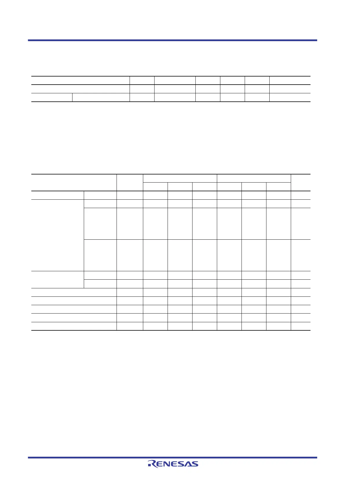
Table 51.55 ROM (Flash Memory for Code Storage) Characteristics (1)
Item Symbol Min. Typ. Max. Unit Test Conditions
Reprogramming/erasure cycle*
1
N
PEC
1000 — — Times
Data hold time After 1000 times of N
PEC
t
DRP
20*
2,
*
3
— — Year T
a
= +85°C
Table 51.56 ROM (Flash Memory for Code Storage) Characteristics (2) High-Speed Operating Mode
Conditions: 2.7 V ≤ VCC = VCC_USB = AVCC0 = VCC_RF = AVCC_RF ≤ 3.6 V, VSS = AVSS0 = VSS_USB = 0 V
Temperature range for the programming/erasure operation: T
a
= –40 to +85°C
Item Symbol
FCLK = 1 MHz FCLK = 32 MHz
Unit
Min. Typ. Max. Min. Typ. Max.
Programming time 8-byte t
P8
— 112 967 — 52.3 491 μs
Erasure time 2-Kbyte t
E2K
— 8.75 278 — 5.50 215 ms
512-Kbyte
(when block
erase
command is
used)
t
E512K
— 928 19218 — 72.0 1679 ms
512-Kbyte
(when all-
block erase
command is
used)
t
EA512K
— 923 19013 — 66.7 1469 ms
Blank check time 8-byte t
BC8
— — 55.0 — — 16.1 μs
2-Kbyte t
BC2K
— — 1840 — — 136 ms
Erase operation forced stop time t
SED
— — 18.0 — — 10.7 μs
Start-up area switching setting time t
SAS
— 12.3 566.5 — 6.2 434 ms
Access window time t
AWS
— 12.3 566.5 — 6.2 434 ms
ROM mode transition wait time 1 t
DIS
2.0 — — 2.0 — — μs
ROM mode transition wait time 2 t
MS
5.0 — — 5.0 — — μs

 Loading...


