R01UH0823EJ0100 Rev.1.00 Page 1506 of 1823
Jul 31, 2019
RX23W Group 43. Capacitive Touch Sensing Unit (CTSU)
43.2.13 CTSU High-Pass Noise Reduction Spectrum Diffusion Control Register
(CTSUSSC)
CTSUSSDIV[3:0] Bits (CTSU Spectrum Diffusion Frequency Division Setting)
These bits specify the spectrum diffusion frequency division setting according to the base clock frequency division
setting. See the relationship between base clock frequencies and CTSUSSDIV[3:0] bits settings in
Table 43.5, for
setting the value of these bits.
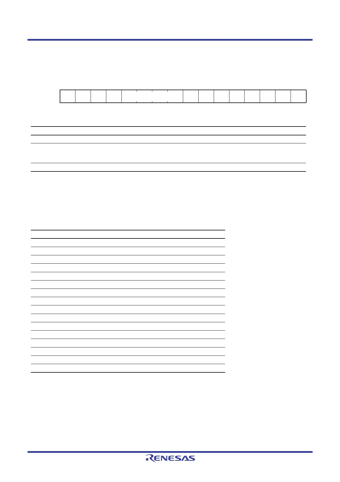
Address(es): CTSU.CTSUSSC 000A 0912h
b15 b14 b13 b12 b11 b10 b9 b8 b7 b6 b5 b4 b3 b2 b1 b0
———— CTSUSSDIV[3:0] ————————
Value after reset:
0000000000000000
Bit Symbol Bit Name Description R/W
b7 to b0 — Reserved These bits are read as 0. The write value should be 0. R/W
b11 to b8 CTSUSSDIV[3:0] CTSU Spectrum Diffusion Frequency
Division Setting
These bits specify the spectrum diffusion frequency
division setting according to the base clock frequency
division setting.
R/W
b15 to b12 — Reserved These bits are read as 0. The write value should be 0. R/W
Table 43.5 Relationship between Base Clock Frequencies and CTSUSSDIV[3:0] Bits Settings
Base Clock Frequency fb (MHz) CTSUSSDIV[3:0] Bits Setting
4.00 ≤ fb 0000b
2.00 ≤ fb < 4.00 0001b
1.33 ≤ fb < 2.00 0010b
1.00 ≤ fb < 1.33 0011b
0.80 ≤ fb < 1.00 0100b
0.67 ≤ fb < 0.80 0101b
0.57 ≤ fb < 0.67 0110b
0.50 ≤ fb < 0.57 0111b
0.44 ≤ fb < 0.50 1000b
0.40 ≤ fb < 0.44 1001b
0.36 ≤ fb < 0.40 1010b
0.33 ≤ fb < 0.36 1011b
0.31 ≤ fb < 0.33 1100b
0.29 ≤ fb < 0.31 1101b
0.27 ≤ fb < 0.29 1110b
fb < 0.27 1111b

 Loading...


