R01UH0823EJ0100 Rev.1.00 Page 1123 of 1823
Jul 31, 2019
RX23W Group 35. I
2
C-bus Interface (RIICa)
35.2.4 I
2
C-bus Mode Register 2 (ICMR2)
Note 1. The DLCS bit setting of 1 (IICφ/2) only becomes valid when SCL pin is low. When SCL pin is high, the DLCS bit setting of 1
becomes invalid and the clock source becomes the internal reference clock (IICφ).
TMOS Bit (Timeout Detection Time Select)
This bit is used to select long mode or short mode for the timeout detection time when the timeout function is enabled
(ICFER.TMOE bit is 1). When this bit is set to 0, long mode is selected. When this bit is set to 1, short mode is selected.
In long mode, the timeout detection internal counter functions as a 16-bit counter. In short mode, the counter functions as
a 14-bit counter. While the SCL0 line is in the state that enables this counter as specified by bits TMOH and TMOL, the
counter counts up in synchronization with the internal reference clock (IICφ) as a count source.
For details on the timeout function, refer to
section 35.11.1, Timeout Function.
TMOL Bit (Timeout L Count Control)
This bit is used to enable or disable the internal counter of the timeout function to count up while the SCL0 line is held
low when the timeout function is enabled (ICFER.TMOE bit is 1).
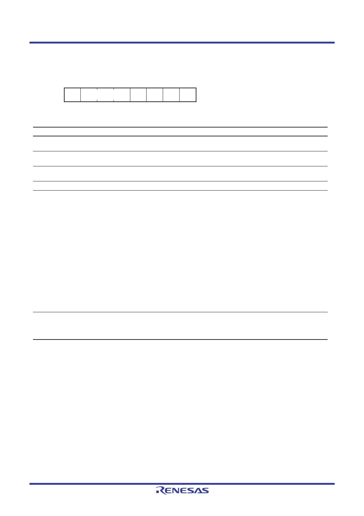
Address(es): RIIC0.ICMR2 0008 8303h
b7 b6 b5 b4 b3 b2 b1 b0
DLCS SDDL[2:0] — TMOH TMOL TMOS
Value after reset:
00000110
Bit Symbol Bit Name Description R/W
b0 TMOS Timeout Detection Time Select 0: Long mode is selected.
1: Short mode is selected.
R/W
b1 TMOL Timeout L Count Control 0: Count-up is disabled while the SCL0 line is at a low level.
1: Count-up is enabled while the SCL0 line is at a low level.
R/W
b2 TMOH Timeout H Count Control 0: Count-up is disabled while the SCL0 line is at a high level.
1: Count-up is enabled while the SCL0 line is at a high level.
R/W
b3 — Reserved This bit is read as 0. The write value should be 0. R/W
b6 to b4 SDDL[2:0] SDA Output Delay Counter
When ICMR2.DLCS bit is 0 (IICφ)
b6 b4
0 0 0: No output delay
0 0 1: 1 IICφ cycle
0 1 0: 2 IICφ cycles
0 1 1: 3 IICφ cycles
1 0 0: 4 IICφ cycles
1 0 1: 5 IICφ cycles
1 1 0: 6 IICφ cycles
1 1 1: 7 IICφ cycles
When ICMR2.DLCS bit is 1 (IICφ/2)
b6 b4
0 0 0: No output delay
0 0 1: 1 or 2 IICφ cycles
0 1 0: 3 or 4 IICφ cycles
0 1 1: 5 or 6 IICφ cycles
1 0 0: 7 or 8 IICφ cycles
1 0 1: 9 or 10 IICφ cycles
1 1 0: 11 or 12 IICφ cycles
1 1 1: 13 or 14 IICφ cycles
R/W
b7 DLCS SDA Output Delay Clock Source
Select
0: The internal reference clock (IICφ) is selected as the clock
source of the SDA output delay counter.
1: The internal reference clock divided by 2 (IICφ/2) is selected as
the clock source of the SDA output delay counter.*
1
R/W

 Loading...


