R01UH0823EJ0100 Rev.1.00 Page 412 of 1823
Jul 31, 2019
RX23W Group 20. Event Link Controller (ELC)
20.2.2 Event Link Setting Register n (ELSRn)
(n = 1 to 4, 7, 8, 10, 12, 14 to 16, 18 to 29)
The ELSRn register specifies an event signal to be linked to for each peripheral module. Table 20.2 shows the
correspondence between the ELSRn register and the peripheral modules.
Table 20.3 shows the correspondence between
values set in the ELSRn register and event signals.
Note 1. Specify an event number to 32h (LPT compare match).
Note 2. Specify an event number from among 63h to 6Ah. Do not set other values.
Note 3. Do not set the DOC data operation condition met signal (6Ah) in the ELSR24, ELSR25, ELSR26, and ELSR27 registers.
Address(es): ELC.ELSR1 0008 B102h, ELC.ELSR2 0008 B103h, ELC.ELSR3 0008 B104h, ELC.ELSR4 0008 B105h, ELC.ELSR7 0008 B108h,
ELC.ELSR8 0008 B109h, ELC.ELSR10 0008 B10Bh, ELC.ELSR12 0008 B10Dh, ELC.ELSR14 0008 B10Fh, ELC.ELSR15 0008 B110h,
ELC.ELSR16 0008 B111h, ELC.ELSR18 0008 B113h, ELC.ELSR19 0008 B114h, ELC.ELSR20 0008 B115h, ELC.ELSR21 0008 B116h,
ELC.ELSR22 0008 B117h, ELC.ELSR23 0008 B118h, ELC.ELSR24 0008 B119h, ELC.ELSR25 0008 B11Ah, ELC.ELSR26 0008 B11Bh,
ELC.ELSR27 0008 B11Ch, ELC.ELSR28 0008 B11Dh, ELC.ELSR29 0008 B11Eh
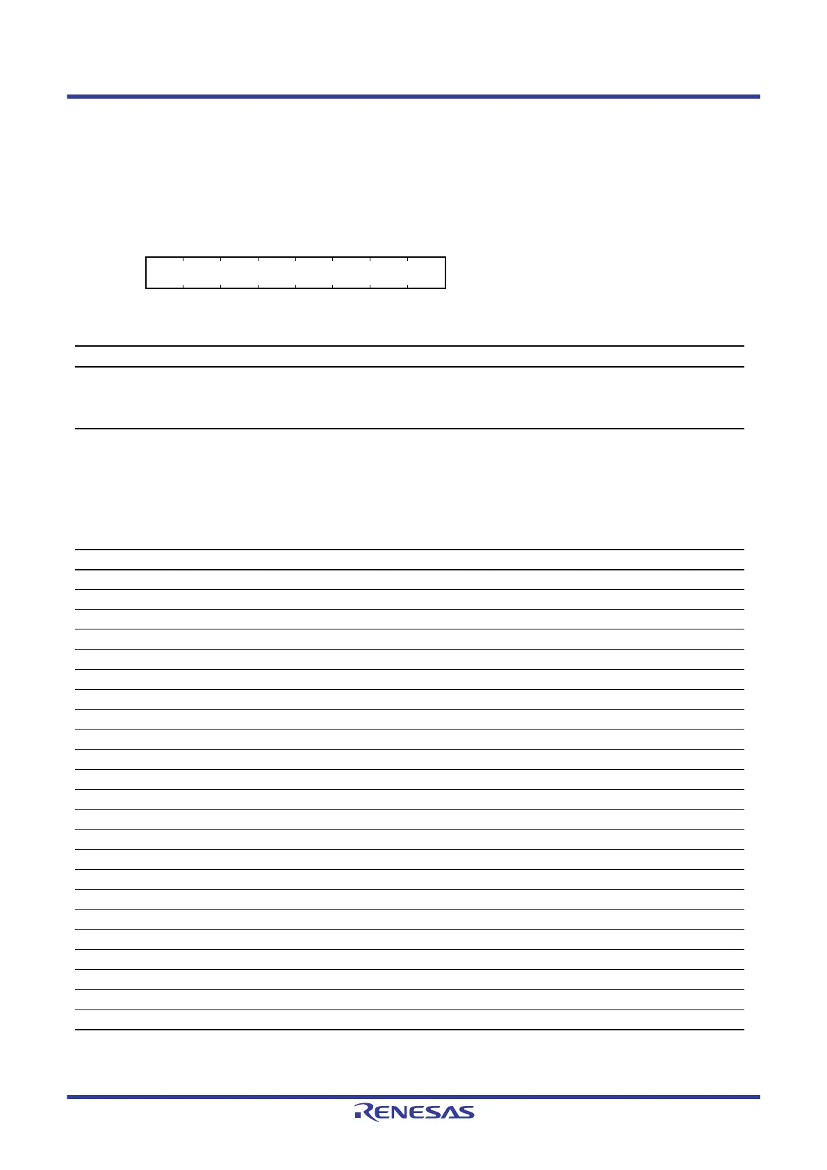
b7 b6 b5 b4 b3 b2 b1 b0
ELS[7:0]
Value after reset:
00000000
Bit Symbol Bit Name Description R/W
b7 to b0 ELS[7:0] Event Link Select 00h: Event signal output to the corresponding peripheral
module is disabled.
08h to 6Ah: Set the number for the event signal to be linked.
Settings other than above are prohibited.
R/W
Table 20.2 Correspondence between the ELSRn Register and the Peripheral Modules
Register Name Peripheral Module
ELSR1 MTU1
ELSR2 MTU2
ELSR3 MTU3
ELSR4 MTU4
ELSR7 CMT1
ELSR8 ICU (LPT dedicated interrupt)*
1
ELSR10 TMR0
ELSR12 TMR2
ELSR14 CTSU
ELSR15 S12AD
ELSR16 DA0
ELSR18 ICU (Interrupt 1)*
2
ELSR19 ICU (Interrupt 2)*
2
ELSR20 Output port group 1
ELSR21 Output port group 2
ELSR22 Input port group 1
ELSR23 Input port group 2
ELSR24 Single port 0*
3
ELSR25 Single port 1*
3
ELSR26 Single port 2*
3
ELSR27 Single port 3*
3
ELSR28 Clock source switching to LOCO
ELSR29 POE

 Loading...


