R01UH0823EJ0100 Rev.1.00 Page 51 of 1823
Jul 31, 2019
RX23W Group
Renesas MCUs
Features
■ 32-bit RXv2 CPU core
Max. operating frequency: 54 MHz
Capable of 88.56 DMIPS in operation at 54 MHz
Enhanced DSP: 32-bit multiply-accumulate and 16-bit
multiply-subtract instructions supported
Built-in FPU: 32-bit single-precision floating point (compliant to
IEEE754)
Divider (fastest instruction execution takes two CPU clock cycles)
Fast interrupt
CISC Harvard architecture with 5-stage pipeline
Variable-length instructions, ultra-compact code
On-chip debugging circuit
Memory protection unit (MPU) supported
■ Low power design and architecture
Operation from a single 1.8-V to 3.6-V supply
RTC capable of operating on the battery backup power supply
Three low power consumption modes
Low power timer (LPT) that operates during the software standby state
■ On-chip flash memory for code
384- to 512-Kbyte capacities
On-board or off-board user programming
Programmable at 1.8 V
For instructions and operands
■ On-chip data flash memory
8 Kbytes (1,000,000 program/erase cycles (typ.))
BGO (Background Operation)
■ On-chip SRAM, no wait states
64-Kbyte size capacities
■ Data transfer functions
DMAC: Incorporates four channels
DTC: Four transfer modes
■ ELC
Module operation can be initiated by event signals without using
interrupts.
Linked operation between modules is possible while the CPU is sleeping.
■ Reset and supply management
Eight types of reset, including the power-on reset (POR)
Low voltage detection (LVD) with voltage settings
■ Clock functions
Main clock oscillator frequency: 1 to 20 MHz
External clock input frequency: Up to 20 MHz
Sub-clock oscillator frequency: 32.768 kHz
Frequency of Bluetooth-dedicated clock oscillator: 32 MHz
PLL circuit input: 4 MHz to 12.5 MHz
On-chip low- and high-speed oscillators, dedicated on-chip low-speed
oscillator for the IWDT
USB-dedicated PLL circuit: 4, 6, 8, or 12 MHz
54 MHz can be set for the system clock and 48 MHz for the USB clock
Generation of a dedicated 32.768-kHz clock for the RTC
Clock frequency accuracy measurement circuit (CAC)
■ Realtime clock
Adjustment functions (30 seconds, leap year, and error)
Calendar count mode or binary count mode selectable
Time capture function
Time capture on event-signal input through external pins
■ Independent watchdog timer
15-kHz on-chip oscillator produces a dedicated clock signal to drive
IWDT operation.
■ Useful functions for IEC60730 compliance
Self-diagnostic and disconnection-detection assistance functions for
the A/D converter, clock frequency accuracy measurement circuit,
independent watchdog timer, RAM test assistance functions using the
DOC, etc.
■ MPC
Input/output functions selectable from multiple pins
■ Up to 12 communication functions
Bluetooth Low Energy (1 channel)
An RF transceiver and link layer compliant with the Bluetooth 5.0 Low
Energy specification
LE 1M PHY, LE 2M PHY, LE Coded PHY (125 kbps and 500 kbps),
and LE Advertising extension support
On-chip Bluetooth-dedicated AES-CCM (128-bit blocks) encryption
circuit
USB 2.0 host/function/On-The-Go (OTG) (one channel),
full-speed = 12 Mbps, low-speed = 1.5 Mbps, isochronous transfer, and
BC (Battery Charger) supported
CAN (one channel) compliant to ISO11898-1:
Transfer at up to 1 Mbps
SCI with many useful functions (up to 4 channels)
Asynchronous mode, clock synchronous mode, smart card interface
Reduction of errors in communications using the bit modulation
function
IrDA interface (one channel, in cooperation with the SCI5)
I
2
C bus interface: Transfer at up to 400 kbps, capable of SMBus
operation (one channel)
RSPI (one channel): Transfer at up to 16 Mbps
Serial sound interface (one channel)
SD host interface (optional: one channel) SD memory/ SDIO 1-bit or
4-bit SD bus supported
■ Up to 19 extended-function timers
16-bit MTU: input capture, output compare, complementary PWM
output, phase counting mode (five channels)
16-bit TPU: input capture, output compare, phase counting mode (six
channels)
8-bit TMR (four channels)
16-bit compare-match timers (four channels)
■ 12-bit A/D converter
Capable of conversion within 0.83 μs
14 channels
Sampling time can be set for each channel
Self-diagnostic function and analog input disconnection detection
assistance function
■ 12-bit D/A converter
Two channels
■ Capacitive touch sensing unit
Self-capacitance method: A single pin configures a single key,
supporting up to 12 keys
Mutual capacitance method: Matrix configuration with 12 pins, supporting
up to 36 keys
■ Analog comparator
Two channels × one unit
■ General I/O ports
5-V tolerant, open drain, input pull-up, switching of driving capacity
■ Encryption functions (TSIP-Lite)
Unauthorized access to the encryption engine is disabled and
imposture and falsification of information are prevented
Safe management of keys
128- or 256-bit key length of AES for ECB, CBC, GCM, others
True random number generator
■ Temperature sensor
■ Operating temperature range
40 to +85C
■ Applications
General industrial and consumer equipment
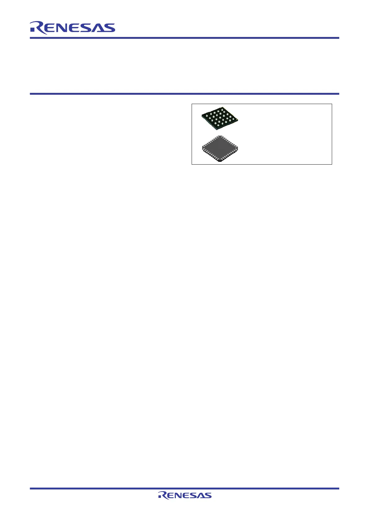
PVQN0056LA-A 7 × 7 mm, 0.4 mm pitch
PTBG0085KB-A 5.5 × 5.5 mm, 0.5 mm pitch
54-MHz 32-bit RX MCUs, built-in FPU, 88.56 DMIPS, up to 512-KB flash memory,
Bluetooth
5.0, various communication functions including USB 2.0 full-speed host/function/OTG, CAN,
SD host interface, serial sound interface, capacitive touch sensing unit, 12-bit A/D converter,
12-bit D/A converter, RTC, Encryption functions
R01UH0823EJ0100
Rev.1.00
Jul 31, 2019
 Loading...


