R01UH0823EJ0100 Rev.1.00 Page 996 of 1823
Jul 31, 2019
RX23W Group 33. Serial Communications Interface (SCIg, SCIh)
33.2.12 Modulation Duty Register (MDDR)
The MDDR register corrects the bit rate adjusted by the BRR register.
When the SEMR.BRME bit is set to 1, the bit rate generated by the on-chip baud rate generator is evenly corrected
according to the settings of the MDDR register (M/256). The relationship between the MDDR register setting (M) and
the bit rate (B) is given in
Table 33.24.
The range of the value that can be set in the MDDR register is from 80h to FFh. A value other than these cannot be set.
The MDDR register is writable only when the TE and RE bits in the SCR register are 0.
B: Bit rate (bps)
M: MDDR setting (128 ≤ MDDR ≤ 256)
N: BRR setting for baud rate generator (0 ≤ N ≤ 255)
PCLK: Operating frequency (MHz)
n and S: Determined by the settings of the SMR and SCMR registers as listed in Table 33.12 and Table 33.13, section
33.2.11, Bit Rate Register (BRR).
Note 1. Do not use this function in clock synchronous mode and in the highest speed settings in simple SPI mode (SMR.CKS[1:0] =
00b, SCR.CKE[1] = 0, and BRR = 0).
Note 2. Adjust the bit rate so that the widths at high and low level of the SCL output in simple I
2
C mode satisfy the I
2
C-bus standard.
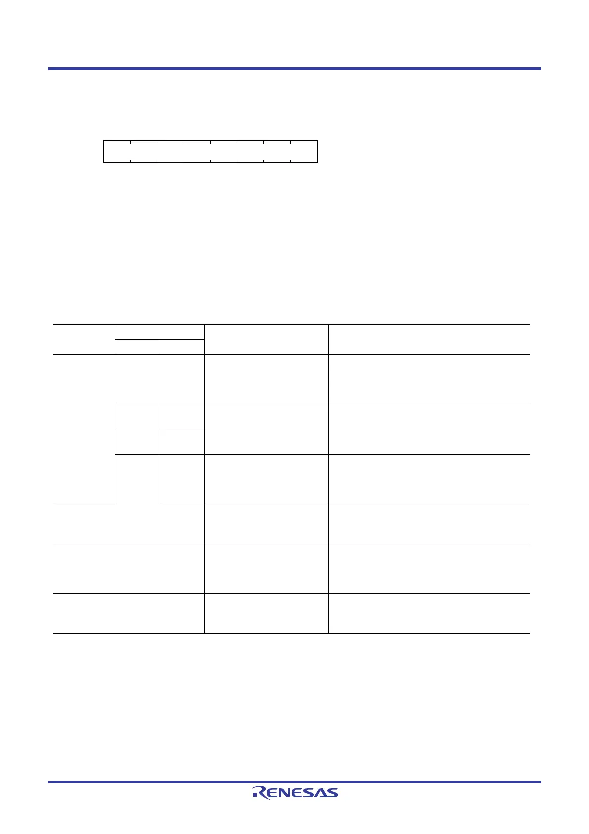
Address(es): SCI1.MDDR 0008 A032h, SCI5.MDDR 0008 A0B2h, SCI8.MDDR 0008 A112h, SCI12.MDDR 0008 B312h
b7 b6 b5 b4 b3 b2 b1 b0
Value after reset:
11111111
Table 33.24 Relationship between MDDR Setting (M) and Bit Rate (B) When Bit Rate Modulation Function is
Used
Mode
SEMR Settings
BRR Setting Error (%)BGDM Bit ABCS Bit
Asynchronous,
multi-processor
communication
00
10
01
11
Clock synchronous, simple SPI*
1
Smart card interface
Simple I
2
C*
2
N
PCLK 10
6
64 2
2n 1–
256
M
----------
B
------------------------------------------------------- 1–=
Error
PCLK 10
6
B64 2
2n 1–
256
M
----------
N1+
-------------------------------------------------------------------------------- 1–
100=
N
PCLK 10
6
32 2
2n 1–
256
M
----------
B
------------------------------------------------------- 1–=
Error
PCLK 10
6
B32 2
2n 1–
256
M
----------
N1+
-------------------------------------------------------------------------------- 1–
100=
N
PCLK 10
6
16 2
2n 1–
256
M
----------
B
------------------------------------------------------- 1–=
Error
PCLK 10
6
B16 2
2n 1–
256
M
----------
N1+
-------------------------------------------------------------------------------- 1–
100=
N
PCLK 10
6
82
2n 1–
256
M
----------
B
---------------------------------------------------- 1–=
N
PCLK 10
6
S2
2n 1+
256
M
----------
B
----------------------------------------------------- 1–=
Error
PCLK 10
6
BS 2
2n 1+
256
M
----------
N1+
------------------------------------------------------------------------------ 1–
100=
N
PCLK 10
6
64 2
2n 1–
256
M
----------
B
------------------------------------------------------- 1–=

 Loading...


