R01UH0823EJ0100 Rev.1.00 Page 1304 of 1823
Jul 31, 2019
RX23W Group 37. Serial Sound Interface (SSI)
37.2 Register Descriptions
37.2.1 Control Register (SSICR)
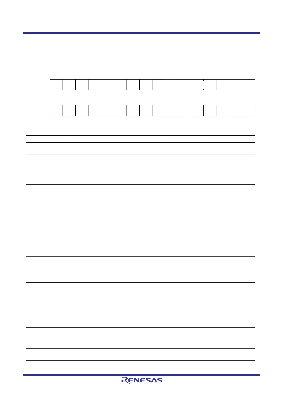
Address(es): SSI0.SSICR 0008 A500h
b31 b30 b29 b28 b27 b26 b25 b24 b23 b22 b21 b20 b19 b18 b17 b16
— CKS TUIEN TOIEN RUIEN ROIEN IIEN — CHNL[1:0] DWL[2:0] SWL[2:0]
Value after reset:
0000000000000000
b15b14b13b12b11b10b9b8b7b6b5b4b3b2b1b0
SCKD SWSD SCKP SWSP SPDP SDTA PDTA DEL CKDV[3:0] MUEN — TEN REN
Value after reset:
0000000000000000
Bit Symbol Bit Name Description R/W
b0 REN Receive Enable 0: Disables receive operation.
1: Enables receive operation.
R/W
b1 TEN Transmit Enable 0: Disables transmit operation.
1: Enables transmit operation.
R/W
b2 — Reserved This bit is read as 0. The write value should be 0. R/W
b3 MUEN Mute Enable*
1
0: Not muted.
1: Muted.
R/W
b7 to b4 CKDV[3:0] Serial Bit Clock Frequency
Setting*
3
b7 b4
0000:MCLK
0001:MCLK/2
0010:MCLK/4
0011:MCLK/8
0100:MCLK/16
0101:MCLK/32
0110:MCLK/64
0111:MCLK/128
1000:MCLK/6
1001:MCLK/12
1010:MCLK/24
1011:MCLK/48
1100:MCLK/96
Settings other than above are prohibited.
R/W
b8 DEL Serial Data Delay*
3
0: I
2
S format compatibility
One clock cycle delay between SSIWS0 and SSITXD0/
SSIRXD0
1: MSB-first left-justified/right-justified format compatibility
No delay between SSIWS0 and SSITXD0/SSIRXD0
R/W
b9 PDTA Parallel Data Allocation*
3
When data word length is 8 or 16 bits:
0: The lower bits of parallel data (SSIFTDR, SSIFRDR) are
transferred prior to the upper bits.
1: The upper bits of parallel data (SSIFTDR, SSIFRDR) are
transferred prior to the lower bits.
When data word length is 18, 20, 22, or 24 bits:
0: Parallel data (SSIFTDR, SSIFRDR) is left-justified.
1: Parallel data (SSIFTDR, SSIFRDR) is right-justified.
R/W
b10 SDTA Serial Data Alignment*
3
0: Transmitting and receiving in the order of serial data and
padding bits
1: Transmitting and receiving in the order of padding bits and
serial data
R/W
b11 SPDP Serial Padding Polarity*
3
0: Padding data is 0.
1: Padding data is 1.
R/W

 Loading...


