R01UH0823EJ0100 Rev.1.00 Page 1116 of 1823
Jul 31, 2019
RX23W Group 35. I
2
C-bus Interface (RIICa)
35.2 Register Descriptions
35.2.1 I
2
C-bus Control Register 1 (ICCR1)
SDAO Bit (SDA Output Control/Monitor) and SCLO Bit (SCL Output Control/Monitor)
These bits are used to directly control the SDA0 and SCL0 signals output from the RIIC.
When writing to these bits, also write 0 to the SOWP bit.
The result of setting these bits is input to the RIIC via the input buffer. When slave mode is selected, a start condition
may be detected and the bus may be released depending on the bit settings.
Do not rewrite these bits during a start condition, stop condition, restart condition, or during transmission or reception.
Operation after rewriting under the above conditions is not guaranteed.
When reading these bits, the state of signals output from the RIIC can be read.
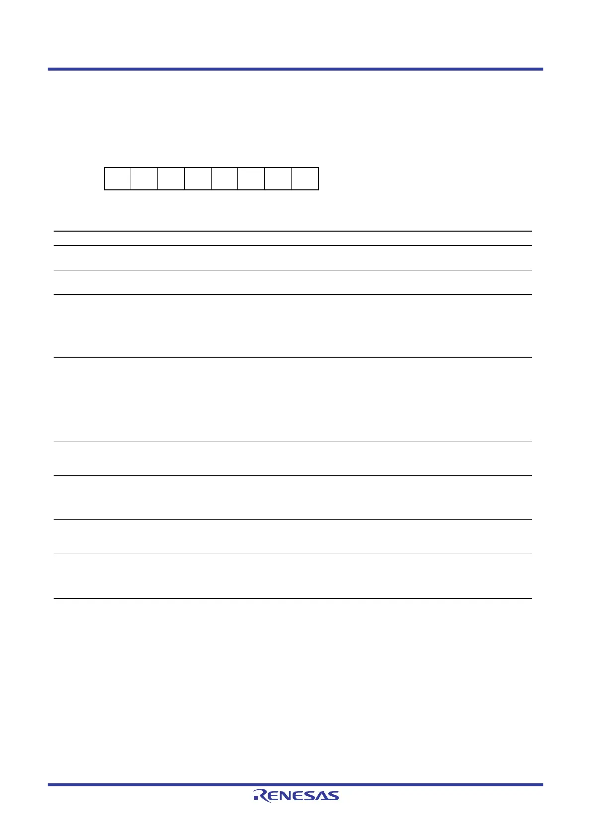
Address(es): RIIC0.ICCR1 0008 8300h
b7 b6 b5 b4 b3 b2 b1 b0
ICE IICRST CLO SOWP SCLO SDAO SCLI SDAI
Value after reset:
00011111
Bit Symbol Bit Name Description
R/W
b0
SDAI SDA Line Monitor 0: SDA0 line is low.
1: SDA0 line is high.
R
b1
SCLI SCL Line Monitor 0: SCL0 line is low.
1: SCL0 line is high.
R
b2
SDAO SDA Output Control/Monitor
Read:
0: The RIIC has driven the SDA0 pin low.
1: The RIIC has released the SDA0 pin.
Write:
0: The RIIC drives the SDA0 pin low.
1: The RIIC releases the SDA0 pin.
R/W
b3
SCLO SCL Output Control/Monitor
Read:
0: The RIIC has driven the SCL0 pin low.
1: The RIIC has released the SCL0 pin.
Write:
0: The RIIC drives the SCL0 pin low.
1: The RIIC releases the SCL0 pin.
(High level output is achieved through an external pull-up
resistor.)
R/W
b4
SOWP SCLO/SDAO Write Protect 0: SCLO and SDAO bits can be written.
1: SCLO and SDAO bits are protected.
(This bit is read as 1.)
R/W
b5
CLO Extra SCL Clock Cycle Output 0: Does not output an extra SCL clock cycle (default).
1: Outputs an extra SCL clock cycle.
(The CLO bit is cleared automatically after one clock cycle is
output.)
R/W
b6
IICRST I
2
C-bus Interface Internal
Reset
0: Releases the RIIC reset or internal reset.
1: Initiates the RIIC reset or internal reset.
(Clears the bit counter and the SCL0/SDA0 output latch)
R/W
b7
ICE I
2
C-bus Interface Enable 0: Disable (SCL0 and SDA0 pins in inactive state)
1: Enable (SCL0 and SDA0 pins in active state)
(Combined with the IICRST bit to select either RIIC or internal
reset.)
R/W

 Loading...


