R01UH0823EJ0100 Rev.1.00 Page 1444 of 1823
Jul 31, 2019
RX23W Group 40. SD Host Interface (SDHIa)
40.2.19 DMA Transfer Enable Register (SDDMAEN)
Note 1. Do not rewrite this bit when the SDSTS2.CBSY bit is 1.
Note 2. When the SDIMSK2.BWEM bit is 0 or the SDIMSK2.BREM bit is 0, set the SDDMAEN.DMAEN bit to 0. When the
SDDMAEN.DMAEN bit is 1, set the SDIMSK2.BWEM bit to 1 and the SDIMSK2.BREM bit to 1.
The SDDMAEN register enables and disables DMA transfer.
DMAEN Bit (DMA Transfer Enable)
When using DMA transfer to access the SD buffer, set the DMAEN bit to 1 before setting the SDCMD register.
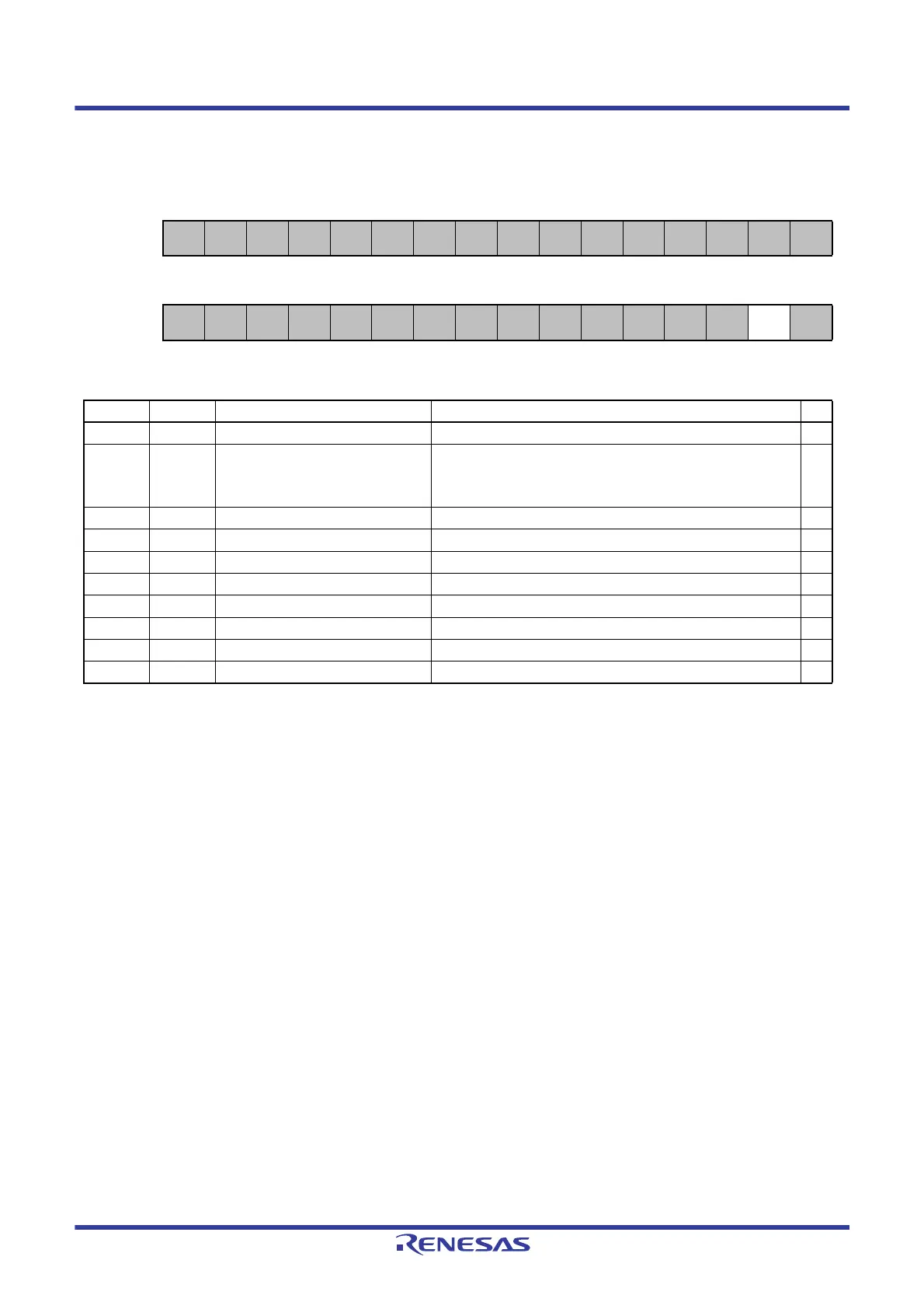
SDDMAEN
Address(es): SDHI.SDDMAEN 0008 ADB0h
b31 b30 b29 b28 b27 b26 b25 b24 b23 b22 b21 b20 b19 b18 b17 b16
— — — — — — — — — — — — — — — —
Value after reset:
0000000000000000
b15 b14 b13 b12 b11 b10 b9 b8 b7 b6 b5 b4 b3 b2 b1 b0
— — — — — — — — — — — — — —
DMAEN
—
Value after reset:
0001000000010000
Bit Symbol Bit Name Description R/W
b0 — Reserved This bit is 0 when read. Set it to 0 when writing. R/W
b1 DMAEN DMA Transfer Enable
*1
*2
0: Using DMAC and DTC to access the SDBUFR register is
disabled
1: Using DMAC and DTC to access the SDBUFR register is
enabled
R/W
b3, b2 — Reserved These bits are 0 when read. Set them to 0 when writing. R
b4 — Reserved This bit is 1 when read. Set it to 1 when writing. R
b5 — Reserved This bit is 0 when read. Set it to 0 when writing. R/W
b7, b6 — Reserved These bits are 0 when read and cannot be modified. R
b9, b8 — Reserved These bits are 0 when read. Set them to 0 when writing. R/W
b11, b10 — Reserved These bits are 0 when read and cannot be modified. R
b12 — Reserved This bit is 1 when read. Set it to 1 when writing. R
b31 to b13 — Reserved These bits are 0 when read and cannot be modified. R

 Loading...


