R01UH0823EJ0100 Rev.1.00 Page 1778 of 1823
Jul 31, 2019
RX23W Group 51. Electrical Characteristics
51.3.5 Timing of On-Chip Peripheral Modules
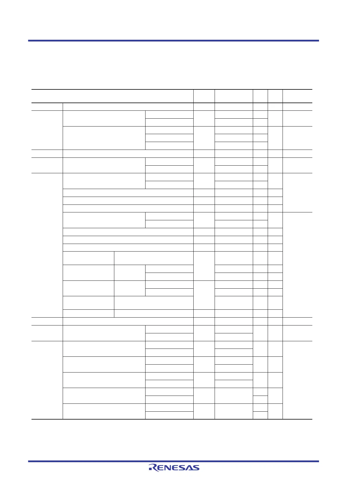
Table 51.32 Timing of On-Chip Peripheral Modules (1)
Conditions: 1.8 V ≤ VCC = VCC_USB = AVCC0 = VCC_RF = AVCC_RF ≤ 3.6 V, VSS = AVSS0 = VSS_USB = VSS_RF = 0 V,
T
a
= –40 to +85°C
Item Symbol Min. Max.
Unit
*1
Test
Conditions
I/O ports Input data pulse width t
PRW
1.5 — t
Pcyc
Figure 51.34
MTU/TPU Input capture input pulse width Single-edge setting t
TICW
1.5 — t
Pcyc
Figure 51.35
Both-edge setting 2.5 —
Timer clock pulse width Single-edge setting t
TCKWH
,
t
TCKWL
1.5 — t
Pcyc
Figure 51.36
Both-edge setting 2.5 —
Phase counting mode 2.5 —
POE POE# input pulse width t
POEW
1.5 — t
Pcyc
Figure 51.37
TMR Timer clock pulse width Single-edge setting t
TMCWH
,
t
TMCWL
1.5 — t
Pcyc
Figure 51.38
Both-edge setting 2.5 —
SCI Input clock cycle time Asynchronous t
Scyc
4—t
Pcyc
Figure 51.39
Clock synchronous 6 —
Input clock pulse width t
SCKW
0.4 0.6 t
Scyc
Input clock rise time t
SCKr
—20ns
Input clock fall time t
SCKf
—20ns
Output clock cycle time Asynchronous t
Scyc
16 — t
Pcyc
Figure 51.40
Clock synchronous 4 —
Output clock pulse width t
SCKW
0.4 0.6 t
Scyc
Output clock rise time t
SCKr
—20ns
Output clock fall time t
SCKf
—20ns
Transmit data delay time
(master)
Clock synchronous t
TXD
—40ns
Transmit data delay time
(slave)
Clock
synchronous
2.7 V or above — 65 ns
1.8 V or above — 100 ns
Receive data setup time
(master)
Clock
synchronous
2.7 V or above t
RXS
65 — ns
1.8 V or above 90 — ns
Receive data setup time
(slave)
Clock synchronous 40 — ns
Receive data hold time Clock synchronous t
RXH
40 — ns
A/D converter Trigger input pulse width t
TRGW
1.5 — t
Pcyc
Figure 51.41
CAC CACREF input pulse width t
Pcyc
≤ t
cac
*2
t
CACREF
4.5 t
cac
+ 3 t
Pcyc
—ns
t
Pcyc
> t
cac
*2
5 t
cac
+ 6.5 t
Pcyc
CLKOUT CLKOUT pin output cycle
*4
VCC = 2.7 V or above t
Ccyc
62.5 — ns Figure 51.42
VCC = 1.8 V or above 125
CLKOUT pin high pulse width
*3
VCC = 2.7 V or above t
CH
15 — ns
VCC = 1.8 V or above 30
CLKOUT pin low pulse width
*3
VCC = 2.7 V or above t
CL
15 — ns
VCC = 1.8 V or above 30
CLKOUT pin output rise time VCC = 2.7 V or above t
Cr
—12ns
VCC = 1.8 V or above 25
CLKOUT pin output fall time VCC = 2.7 V or above t
Cf
—12ns
VCC = 1.8 V or above 25

 Loading...


