R01UH0823EJ0100 Rev.1.00 Page 1281 of 1823
Jul 31, 2019
RX23W Group 36. CAN Module (RSCAN)
36.8 RAM Window
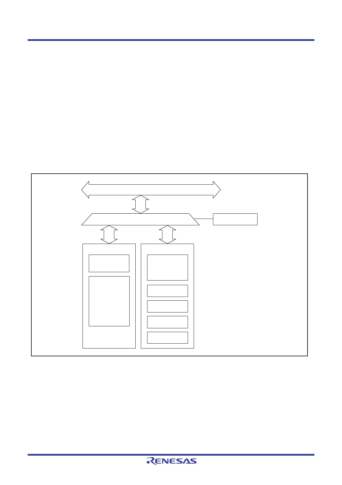
The CAN area from 000A 83A0h to 000A 8681h consists of two windows. The GRWCR.RPAGE bit is used to switch
the allocation of registers.
Registers allocated when the GRWCR.RPAGE bit is set to 0 (window 0 selected)
Receive rule entry registers: GAFLIDLj, GAFLIDHj, GAFLMLj, GAFLMHj, GAFLPLj, GAFLPHj
RAM test registers: RPGACCr
Registers allocated when the GRWCR.RPAGE bit is set to 1 (window 1 selected)
Receive buffer registers: RMIDLn, RMIDHn, RMTSn, RMPTRn, RMDF0n to RMDF3n
Receive FIFO access registers: RFIDLm, RFIDHm, RFTSm, RFPTRm, RFDF0m to RFDF3m
Transmit/receive FIFO access registers: CFIDL0, CFIDH0, CFTS0, CFPTR0, CFDF00 to CFDF30
Transmit buffer registers: TMIDLp, TMIDHp, TMPTRp, TMDF0p to TMDF3p
Transmit history buffer access register: THLACC0
Figure 36.15 RAM Window
RAM test registers
Receive rule
entry registers
RAM window select bit
Window 0
Transmit/receive
FIFO access registers
Transmit history
buffer access register
Receive buffer
registers
Receive FIFO
access registers
Transmit buffer
registers
Window 1
Internal peripheral bus
01

 Loading...


