R01UH0823EJ0100 Rev.1.00 Page 1010 of 1823
Jul 31, 2019
RX23W Group 33. Serial Communications Interface (SCIg, SCIh)
33.2.24 Control Register 3 (CR3)
SDST Bit (Start Frame Detection Start)
Detection of a Start Frame begins when this bit is set to 1. The bit is read as 0.
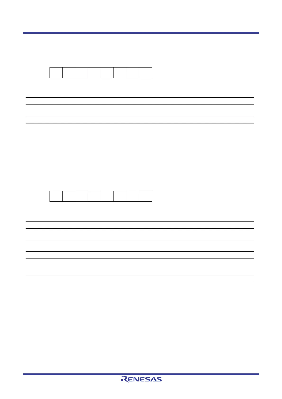
33.2.25 Port Control Register (PCR)
SHARPS Bit (TXDX12/RXDX12 Pin Multiplexing Select)
When this bit is set to 1, the TXDX12 and RXDX12 signals are multiplexed on the same pin so that half-duplex
communications become possible.
Address(es): SCI12.CR3 0008 B324h
b7 b6 b5 b4 b3 b2 b1 b0
———————SDST
Value after reset:
00000000
Bit Symbol Bit Name Description R/W
b0 SDST Start Frame Detection Start 0: Detection of Start Frame is not performed.
1: Detection of Start Frame is performed.
R/W
b7 to b1 — Reserved These bits are read as 0. The write value should be 0. R/W
Address(es): SCI12.PCR 0008 B325h
b7 b6 b5 b4 b3 b2 b1 b0
———
SHARP
S
——
RXDXP
S
TXDXP
S
Value after reset:
00000000
Bit Symbol Bit Name Description R/W
b0 TXDXPS TXDX12 Signal Polarity Select 0: The polarity of TXDX12 signal is not inverted for output.
1: The polarity of TXDX12 signal is inverted for output.
R/W
b1 RXDXPS RXDX12 Signal Polarity
Select
0: The polarity of RXDX12 signal is not inverted for input.
1: The polarity of RXDX12 signal is inverted for input.
R/W
b3, b2 — Reserved These bits are read as 0. The write value should be 0. R/W
b4 SHARPS TXDX12/RXDX12 Pin
Multiplexing Select
0: The TXDX12 and RXDX12 pins are independent.
1: The TXDX12 and RXDX12 signals are multiplexed on the same
pin.
R/W
b7 to b5 — Reserved These bits are read as 0. The write value should be 0. R/W

 Loading...


