R01UH0823EJ0100 Rev.1.00 Page 666 of 1823
Jul 31, 2019
RX23W Group 25. 16-Bit Timer Pulse Unit (TPUa)
ICSELD Bit (TGRD Input Capture Input Select)
Selects the input capture input for TPUm.TGRD (m = 3).
This function allows measurement of high-level width and period of the input pulse on a TIOCCn input pin.
25.2.3 Timer I/O Control Register (TIORH, TIORL, TIOR)
TPU0.TIORH, TPU1.TIOR, TPU2.TIOR, TPU3.TIORH, TPU4.TIOR, TPU5.TIOR
Note 1. If the IOn[3:0] bit (n = A, B) values are changed to output disabled (0000b or 0100b) during low/high/toggle output on compare
match, the TIOCAn/TIOCBn pin (n = 0 to 5) is placed in high impedance state.
Note 2. In TPU0, TPU1, TPU2, and TPU5, which have no TIOCAn pin, these bits are reserved. These bits are read as 0. The write value
should be 0.
TPU3.TIORL
Note 1. If the IOn[3:0] bit (n = C, D) values are changed to output disabled (0000b or 0100b) during low/high/toggle output on compare
match, the TIOCCn/TIOCDn pin (n = 0, 3) is placed in high impedance state.
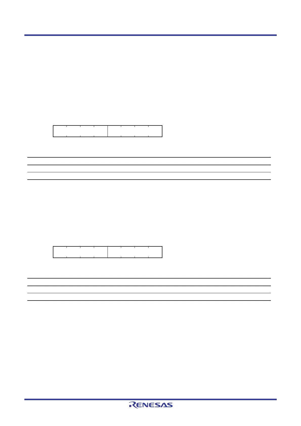
Address(es): TPU0.TIORH 0008 8112h, TPU1.TIOR 0008 8122h, TPU2.TIOR 0008 8132h,
TPU3.TIORH 0008 8142h, TPU4.TIOR 0008 8152h, TPU5.TIOR 0008 8162h
b7 b6 b5 b4 b3 b2 b1 b0
IOB[3:0] IOA[3:0]
Value after reset:
00000000
Bit Symbol Bit Name Description R/W
b3 to b0 IOA[3:0] TGRA Control*
2
See Table 25.13 to Table 25.18.*
1
R/W
b7 to b4 IOB[3:0] TGRB Control See Table 25.13 to Table 25.18.*
1
R/W
Address(es): TPU3.TIORL 0008 8143h
b7 b6 b5 b4 b3 b2 b1 b0
IOD[3:0] IOC[3:0]
Value after reset:
00000000
Bit Symbol Bit Name Description R/W
b3 to b0 IOC[3:0] TGRC Control See Table 25.16.*
1
R/W
b7 to b4 IOD[3:0] TGRD Control See Table 25.16.*
1
R/W

 Loading...


