R01UH0823EJ0100 Rev.1.00 Page 205 of 1823
Jul 31, 2019
RX23W Group 9. Clock Generation Circuit
9.9 Usage Notes
9.9.1 Notes on Clock Generation Circuit
(1) The frequencies of the system clock (ICLK), peripheral module clocks (PCLKA, PCLKB, and PCLKD), and
FlashIF clock (FCLK) supplied to each module can be selected by the SCKCR register. Each frequency should meet
the following:
Select each frequency that is within the operation guaranteed range of clock cycle time (tcyc) specified in AC
characteristics of electrical characteristics.
The frequencies must not exceed the ranges listed in
Table 9.1.
The peripheral modules operate on the PCLKA, PCLKB and PCLKD. Note therefore that the operating speed of
modules such as the timer and SCI varies before and after the frequency is changed.
(2) The relationship of frequencies of the system clock (ICLK), peripheral module clocks A, B, and D (PCLKA,
PCLKB, and PCLKD), and FlashIF clock (FCLK) must be set as follows.
ICLK:FCLK = N:1 or 1:N (N is an integer)
ICLK:PCLKA, PCLKB, and PCLKD = N:1 or 1:N (N is an integer)
(3) To secure the processing after the clock frequency is changed, modify the pertinent clock control register to change
the frequency, and then read the value from the register, and then perform the subsequent processing.
9.9.2 Notes on Resonator
Since various resonator characteristics relate closely to the user's board design, adequate evaluation is required on the
user side before use, referencing the resonator connection example shown in this section. The circuit constants for the
resonator depend on the resonator to be used and the stray capacitance of the mounting circuit. Therefore, the circuit
constants should be determined in full consultation with the resonator manufacturer. The voltage to be applied between
the resonator pins must be within the absolute maximum rating.
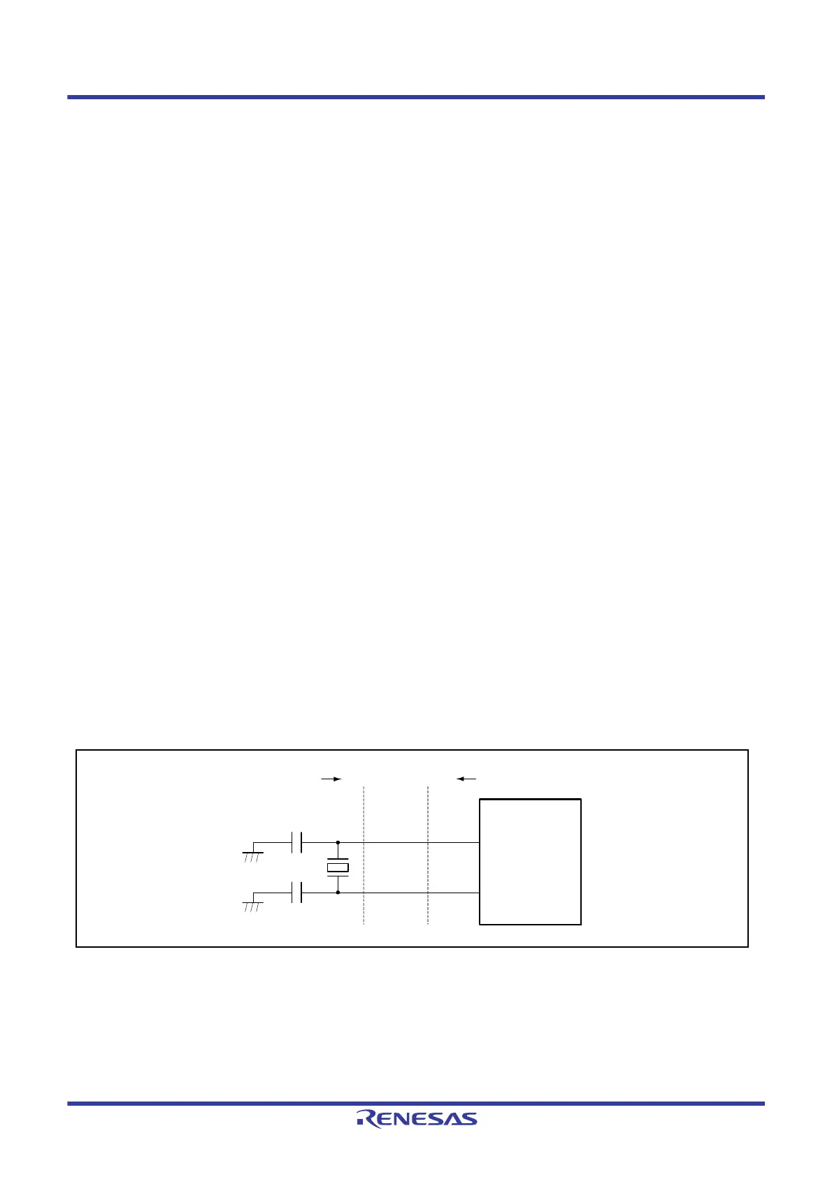
9.9.3 Notes on Board Design
When using a crystal, place the resonator and its load capacitors as close to the XTAL and EXTAL pins as possible.
Other signal lines should be routed away from the oscillation circuit as shown in
Figure 9.13 to prevent electromagnetic
induction from interfering with correct oscillation.
Figure 9.13 Point for Caution on Board Design for the Oscillation Circuit (Applicable to the Main Clock
Oscillator as well as the Sub Clock Oscillator and Bluetooth-Dedicated Osillator)
EXTAL
XTAL
C
L2
C
L1
MCU
Prohibited Signal A Signal B
Prohibited

 Loading...


