R01UH0823EJ0100 Rev.1.00 Page 174 of 1823
Jul 31, 2019
RX23W Group 9. Clock Generation Circuit
9.2.2 System Clock Control Register 3 (SCKCR3)
Note: Set the PRCR.PRC0 bit to 1 (write enabled) before rewriting this register.
Note 1. Do not select a clock of frequency higher than 32 MHz when divided by 1 is selected by SCKCR.ICK and MEMWAIT.MEMWAIT
= 0.
This register cannot be rewritten while the flash memory is being programmed or erased.
CKSEL[2:0] Bits (Clock Source Select)
These bits select the source of the system clock (ICLK), peripheral module clock (PCLKA, PCLKB, and PCLKD),
FlashIF clock (FCLK), and USB clock (UCLK) from low-speed on-chip oscillator (LOCO), high-speed on-chip
oscillator (HOCO), the main clock oscillator, the sub-clock oscillator, and the PLL circuit.
Transitions to clock sources which are not in operation are prohibited.
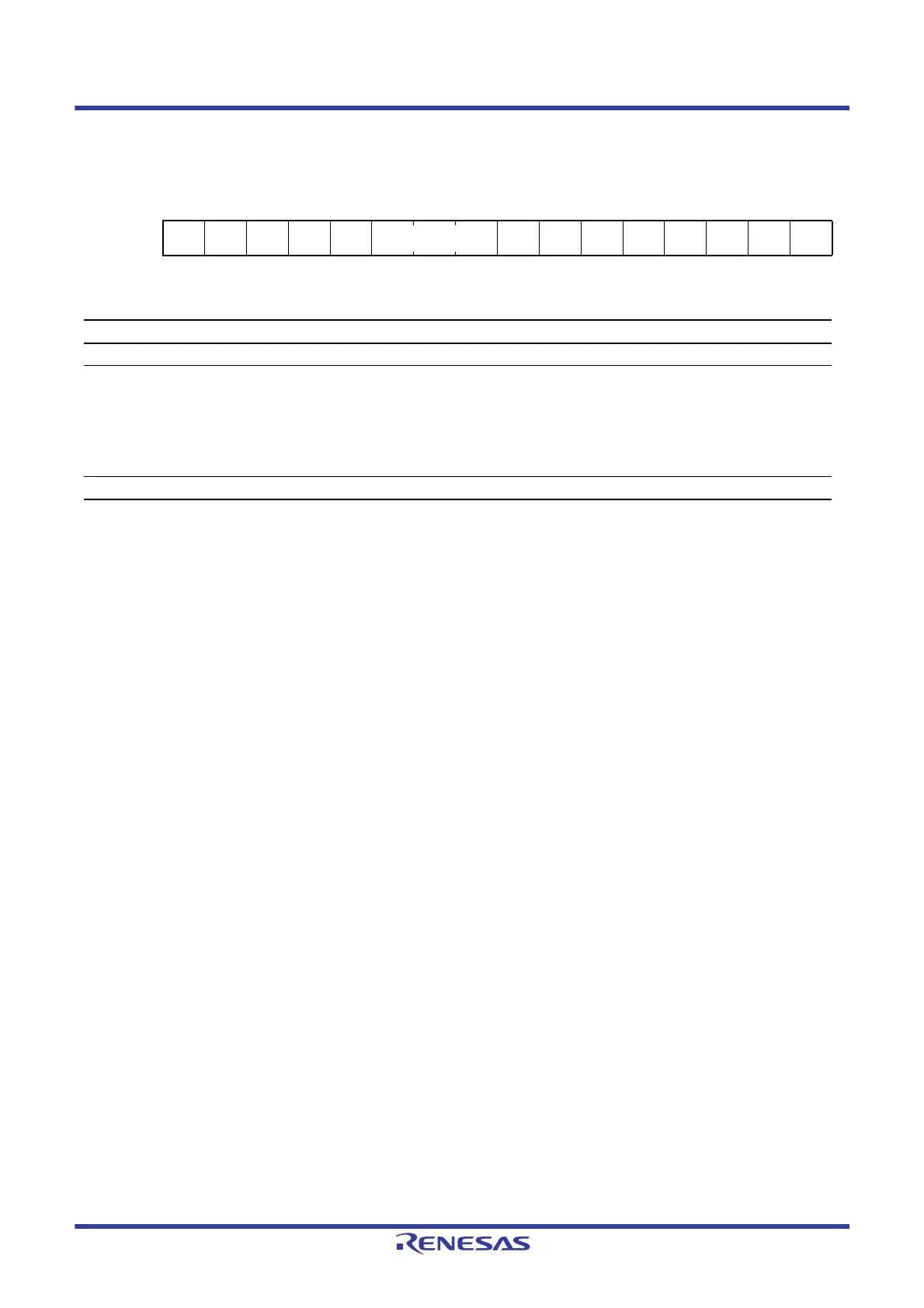
Address(es): 0008 0026h
b15 b14 b13 b12 b11 b10 b9 b8 b7 b6 b5 b4 b3 b2 b1 b0
————— CKSEL[2:0] ————————
Value after reset:
0000000000000000
Bit Symbol Bit Name Description R/W
b7 to b0 — Reserved These bits are read as 0. The write value should be 0. R/W
b10 to b8 CKSEL[2:0]
*
1
Clock Source Select
b10 b8
0 0 0: LOCO
0 0 1: HOCO
0 1 0: Main clock oscillator
0 1 1: Sub-clock oscillator
1 0 0: PLL circuit
Settings other than above are prohibited.
R/W
b15 to b11 — Reserved These bits are read as 0. The write value should be 0. R/W

 Loading...


