R01UH0823EJ0100 Rev.1.00 Page 1426 of 1823
Jul 31, 2019
RX23W Group 40. SD Host Interface (SDHIa)
40.2.6 SD Status Register 1 (SDSTS1)
Note 1. The flag does not change even if set to 1. Writing 0 changes the flag value to 0.
Note 2. The flag changes when the pin level continues for the period set in the SDOPT.CTOP[3:0] bits or longer.
The SDSTS1 register indicates the detection of a response end or access end for a command sequence. The SDSTS1
register also indicates the detection SD card insertion/removal, and indicates the write protection status.
During a multi-block transfer sequence, if CMD12 or CMD52 (SDIO abort) is issued, the ACEND flag becomes 1, but
the RSPEND flag remains set to 0.
If the command sequence is stopped due to a communication error or timeout, the ACEND flag or RSPEND flag
becomes 1.
After a reset is released, the SDD3MON flag, SDD3IN flag, and SDD3RM flag values are changed according to the
status of the SDHI_D3 pin, and their values are changed when data is being transferred in wide bus mode.
Flags to be cleared should be set to 0; flags not being cleared should be set to 1.
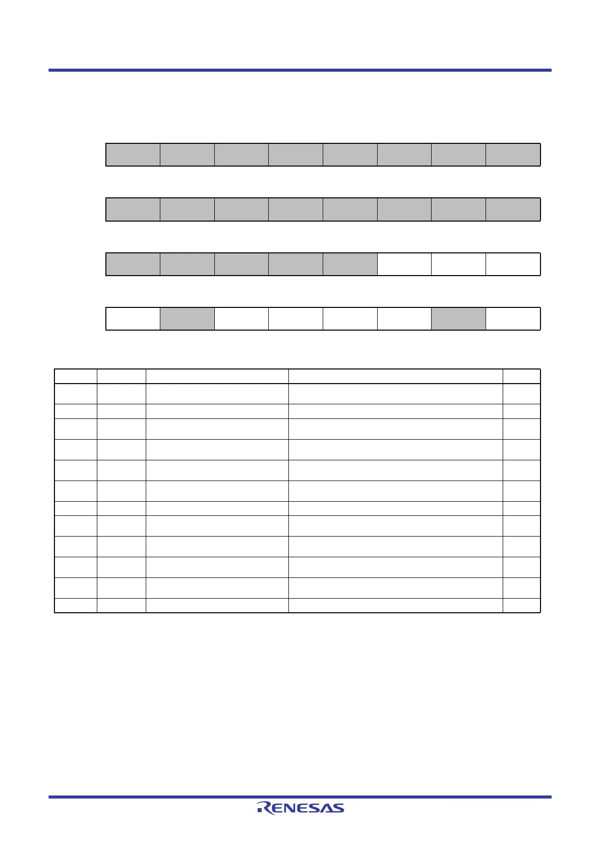
SDSTS1
Address(es): SDHI.SDSTS1 0008 AC38h
b31 b30 b29 b28 b27 b26 b25 b24
— — — — — — — —
Value after reset:
00000000
b23 b22 b21 b20 b19 b18 b17 b16
— — — — — — — —
Value after reset:
00000000
b15 b14 b13 b12 b11 b10 b9 b8
— — — — — SDD3MON SDD3IN SDD3RM
Value after reset:
00000x00
b7 b6 b5 b4 b3 b2 b1 b0
SDWPMON — SDCDMON SDCDIN SDCDRM ACEND — RSPEND
Value after reset:
x0x00000
Bit Symbol Bit Name Description R/W
b0 RSPEND Response End Detection Flag
0: Response end is not detected
1: Response end is detected
R/(W)
*1
b1 — Reserved This bit is 0 when read and cannot be modified. R
b2 ACEND Access End Detection Flag
0: Access end is not detected
1: Access end is detected
R/(W)
*1
b3 SDCDRM SDHI_CD Removal Flag
0: SD card removal not detected by the SDHI_CD pin
1: SD card removal detected by the SDHI_CD pin
R/(W)
*1
b4 SDCDIN SDHI_CD Insertion Flag
0: SD card insertion not detected by the SDHI_CD pin
1: SD card insertion detected by the SDHI_CD pin
R/(W)
*1
b5 SDCDMON SDHI_CD Pin Monitor Flag
0: SDHI_CD pin level is high
*2
1: SDHI_CD pin level is low
*2
R
b6 — Reserved This bit is 0 when read and cannot be modified. R
b7 SDWPMON SDHI_WP Pin Monitor Flag
0: SDHI_WP pin level is high
1: SDHI_WP pin level is low
R
b8 SDD3RM SDHI_D3 Removal Flag
0: SD card removal not detected by the SDHI_D3 pin
1: SD card removal detected by the SDHI_D3 pin
R/(W)
*1
b9 SDD3IN SDHI_D3 Insertion Flag
0: SD card insertion not detected by the SDHI_D3 pin
1: SD card insertion detected by the SDHI_D3 pin
R/(W)
*1
b10 SDD3MON SDHI_D3 Pin Monitor Flag
0: SDHI_D3 pin level is low
1: SDHI_D3 pin level is high
R
b31 to b11 — Reserved These bits are 0 when read and cannot be modified. R

 Loading...


