R01UH0823EJ0100 Rev.1.00 Page 1435 of 1823
Jul 31, 2019
RX23W Group 40. SD Host Interface (SDHIa)
40.2.10 SDHI Clock Control Register (SDCLKCR)
Note 1. Bits CLKSEL[7:0] and CLKEN cannot be write accessed when the SDSTS2.SDCLKCREN flag is 0.
Note 2. When setting the CLKSEL[7:0] bits to 11111111b or when changing the CLKSEL[7:0] bit values from 11111111b to another
value, perform the following steps:
(1) Set the CLKEN bit to 0. Do not change the other bit values.
(2) Change the CLKSEL[7:0] bit values. Do not change the other bit values.
(3) Set the CLKEN bit to 1. Do not change the other bit values.
The SDCLKCR register controls the SDHI clock frequency settings and output. Set the CLKEN bit to 1 before writing to
the SDCMD register to start a command sequence. Do not write access the SDCLKCR register when the
SDSTS2.SDCLKCREN flag is 0.
CLKCTRLEN Bit (SDHI Clock Output Automatic Control Select)
The SDHI clock output automatic control is a function for starting and stopping SDHI clock output only during a
command sequence. When this function is enabled, the SDHI starts outputting the SDHI clock after a value is set to the
SDCMD register. After the command sequence is complete and eight cycles of the SDHI clock elapse, the SDHI stops
outputting the SDHI clock. When the SDCLKCR.CLKEN bit is 0, output from the SDHI_CLK pin becomes low
regardless of the CLKCTRLEN bit setting.
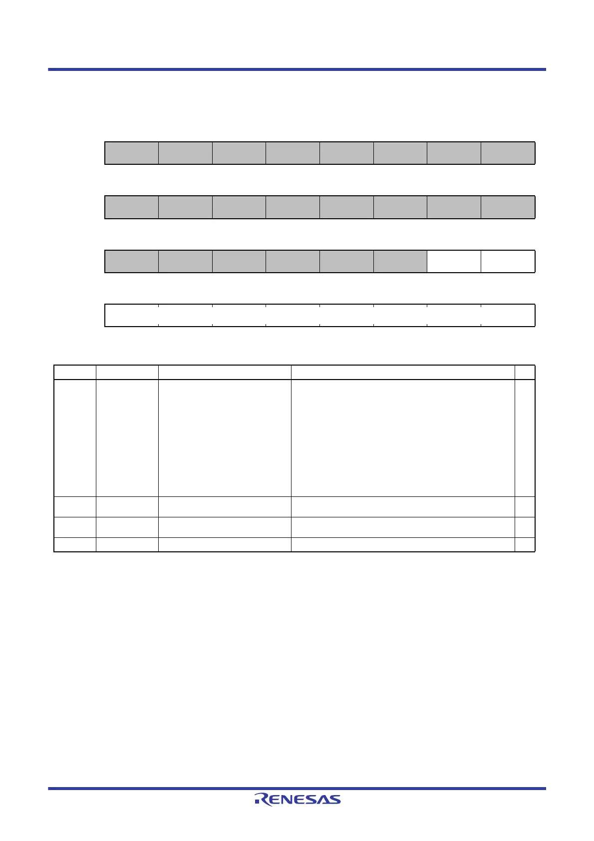
SDCLKCR
Address(es): SDHI.SDCLKCR 0008 AC48h
b31 b30 b29 b28 b27 b26 b25 b24
— — — — — — — —
Value after reset:
00000000
b23 b22 b21 b20 b19 b18 b17 b16
— — — — — — — —
Value after reset:
00000000
b15 b14 b13 b12 b11 b10 b9 b8
— — — — — — CLKCTRLEN CLKEN
Value after reset:
00000000
b7 b6 b5 b4 b3 b2 b1 b0
CLKSEL[7:0]
Value after reset:
00100000
Bit Symbol Bit Name Description R/W
b7 to b0 CLKSEL[7:0] SDHI Clock Frequency Select
*1
b7 b0
0 0 0 0 0 0 0 0: PCLKB divided by 2
0 0 0 0 0 0 0 1: PCLKB divided by 4
0 0 0 0 0 0 1 0: PCLKB divided by 8
0 0 0 0 0 1 0 0: PCLKB divided by 16
0 0 0 0 1 0 0 0: PCLKB divided by 32
0 0 0 1 0 0 0 0: PCLKB divided by 64
0 0 1 0 0 0 0 0: PCLKB divided by 128
0 1 0 0 0 0 0 0: PCLKB divided by 256
1 0 0 0 0 0 0 0: PCLKB divided by 512
1 1 1 1 1 1 1 1: PCLKB
*2
Only set the values listed above.
R/W
b8 CLKEN SDHI Clock Output Control
*1
0: SDHI clock output is disabled (SDHI_CLK signal fixed low)
1: SDHI clock output enabled
R/W
b9 CLKCTRLEN
SDHI Clock Output Automatic
Control Select
0: Automatic control of SDHI clock output disabled
1: Automatic control of SDHI clock output enabled
R/W
b31 to b10 — Reserved These bits are 0 when read and cannot be modified. R

 Loading...


