R01UH0823EJ0100 Rev.1.00 Page 464 of 1823
Jul 31, 2019
RX23W Group 22. Multi-Function Pin Controller (MPC)
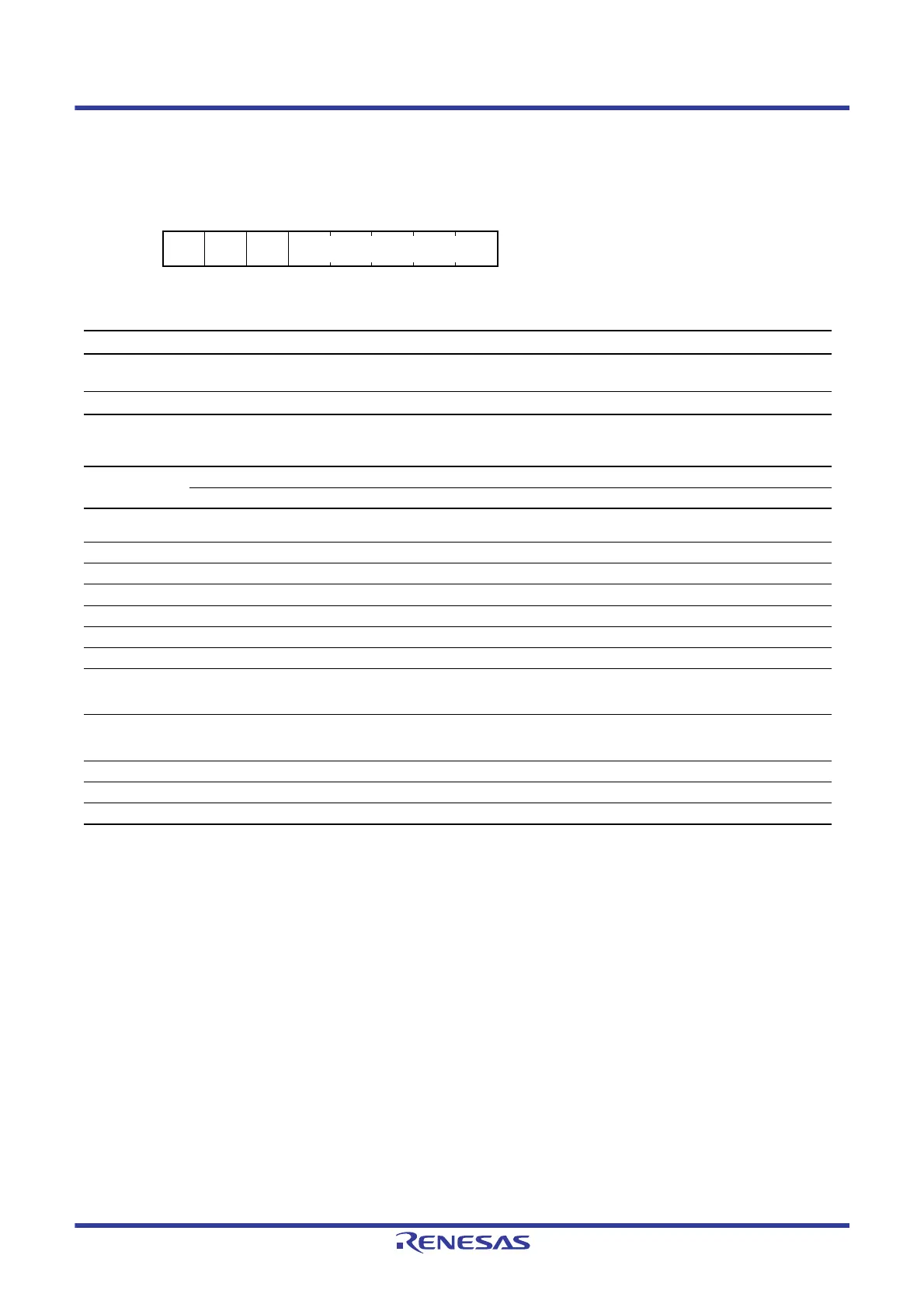
22.2.8 PCn Pin Function Control Registers (PCnPFS) (n = 0, 2 to 7)
—: Do not specify this value.
Note 1. This setting is not supported by 56-pin products.
Address(es): PC0PFS 0008 C1A0h, PC2PFS 0008 C1A2h, PC3PFS 0008 C1A3h,
PC4PFS 0008 C1A4h, PC5PFS 0008 C1A5h, PC6PFS 0008 C1A6h, PC7PFS 0008 C1A7h
b7 b6 b5 b4 b3 b2 b1 b0
— — — PSEL[4:0]
Value after reset:
00000000
Bit Symbol Bit Name Description R/W
b4 to b0 PSEL[4:0] Pin Function Select These bits select the peripheral function. For individual pin functions,
see the tables below.
R/W
b7 to b5 — Reserved These bits are read as 0. The write value should be 0. R/W
Table 22.9 Register Settings for Input/Output Pin Function in 85-Pin and 56-Pin
PSEL[4:0]
Settings
Pin
PC0 PC2 PC3 PC4 PC5 PC6 PC7
00000b
(initial value)
Hi-Z
00001b MTIOC3C MTIOC4B MTIOC4D MTIOC3D MTIOC3B MTIOC3C MTIOC3A
00010b — — — MTCLKC MTCLKD MTCLKA MTCLKB
00011b TCLKC TCLKA TCLKB — — — —
00101b — — — TMCI1 TMRI2 TMCI2 TMO2
00111b — — — POE0# — — CACREF
10001b — — — — USB0_ID USB0_EXICEN —
01010b — RXD5
SMISO5
SSCL5
TXD5
SMOSI5
SSDA5
SCK5 SCK8 RXD8
SMISO8
SSCL8
TXD8
SMOSI8
SSDA8
01011b CTS5#
RTS5#
SS5#
— — CTS8#
RTS8#
SS8#
———
01101b SSLA1 SSLA3 — SSLA0 RSPCKA MOSIA MISOA
11001b TS35 TS30 TS27 TSCAP TS23 TS22 —
11010b — SDHI_D3*
1
SDHI_D0*
1
SDHI_D1*
1
———

 Loading...


