R01UH0823EJ0100 Rev.1.00 Page 1668 of 1823
Jul 31, 2019
RX23W Group 50. Flash Memory (FLASH)
50.4.7 Flash Reset Register (FRESETR)
FRESET Bit (Flash Reset)
When this bit is set to 1, registers FASR, FSARH, FSARL, FEARH, FEARL, FWB0, FWB1, FWB2, FWB3, FCR, and
FEXCR are reset. Also, the values of registers FEAMH and FEAML are undefined. Do not access these registers during
a reset. To release the reset, set this bit to 0.
Do not write to this register while executing a software command or rewriting the extra area.
50.4.8 Flash Area Select Register (FASR)
Data can be written to the FASR register in ROM P/E mode or E2 DataFlash P/E mode.
This register is initialized by a reset or setting the FRESETR.FRESET bit to 1.
Data cannot be written to this register while the FRESETR.FRESET bit is 1.
EXS Bit (Extra Area Select)
Set this bit to 1 before issuing a software command (start-up area information program or access window information
program) for the extra area. Set this bit to 0 before issuing a software command (program, blank check, block erase, or
all-block erase) for the user area.
After issuing a software command, do not change the value until changing it for issuing the next software command.
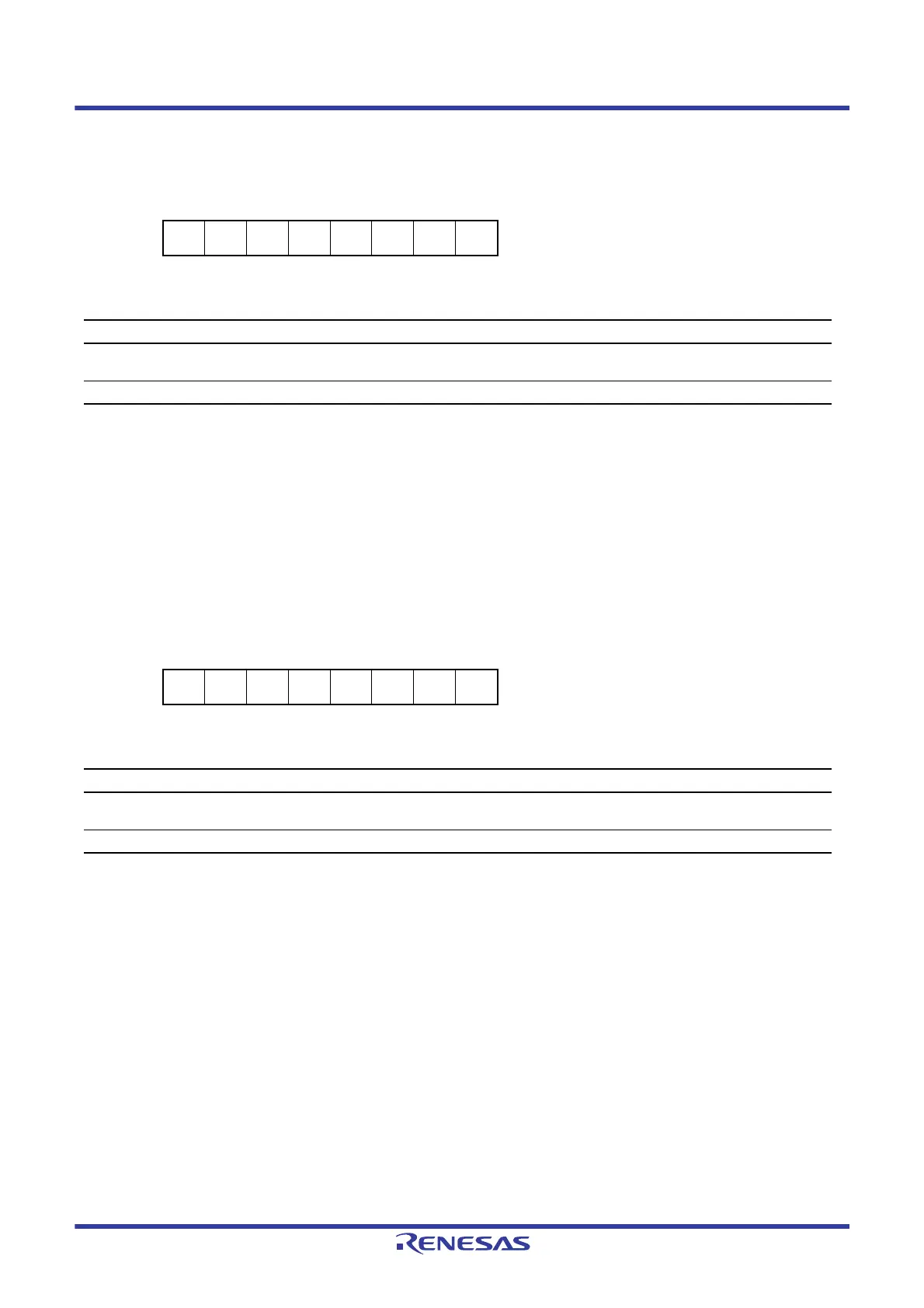
Address(es): FLASH.FRESETR 007F C124h
b7 b6 b5 b4 b3 b2 b1 b0
———————
FRESE
T
Value after reset:
00000000
Bit Symbol Bit Name Description R/W
b0 FRESET Flash Reset 0: Flash control circuit reset is released.
1: Flash control circuit is reset.
R/W
b7 to b1 — Reserved These bits are read as 0. The write value should be 0. R/W
Address(es): FLASH.FASR 007F C104h
b7 b6 b5 b4 b3 b2 b1 b0
———————EXS
Value after reset:
00000000
Bit Symbol Bit Name Description R/W
b0 EXS Extra Area Select 0: User area or data area
1: Extra area
R/W
b7 to b1 — Reserved These bits are read as 0. The write value should be 0. R/W

 Loading...


