R01UH0823EJ0100 Rev.1.00 Page 1621 of 1823
Jul 31, 2019
RX23W Group 45. 12-Bit D/A Converter (R12DAA)
Table 45.2 lists the pin configuration of the 12-bit D/A converter.
45.2 Register Descriptions
45.2.1 D/A Data Register m (DADRm) (m = 0, 1)
The DADRm register is a 16-bit readable/writable register, which stores data to which D/A conversion is to be
performed. Whenever an analog output is enabled, the values in DADRm are converted and output from the D/A
converter.
12-bit data can be relocated by setting the DADPR.DPSEL bit.
Bits “—” are read as 0. The write value should be 0.
Table 45.2 Pin Configuration of 12-Bit D/A Converter
Pin Name I/O Function
AVCC0 Input Analog voltage supply pin for the 12-bit A/D converter and 12-bit D/A converter. Connect this
pin to VCC when not using the 12-bit A/D converter and 12-bit D/A converter.
AVSS0 Input Analog ground pin for the 12-bit A/D converter and 12-bit D/A converter. Connect this pin to
VSS when not using the 12-bit A/D converter and 12-bit D/A converter.
DA0 Output Channel 0 analog output pin
DA1 Output Channel 1 analog output pin
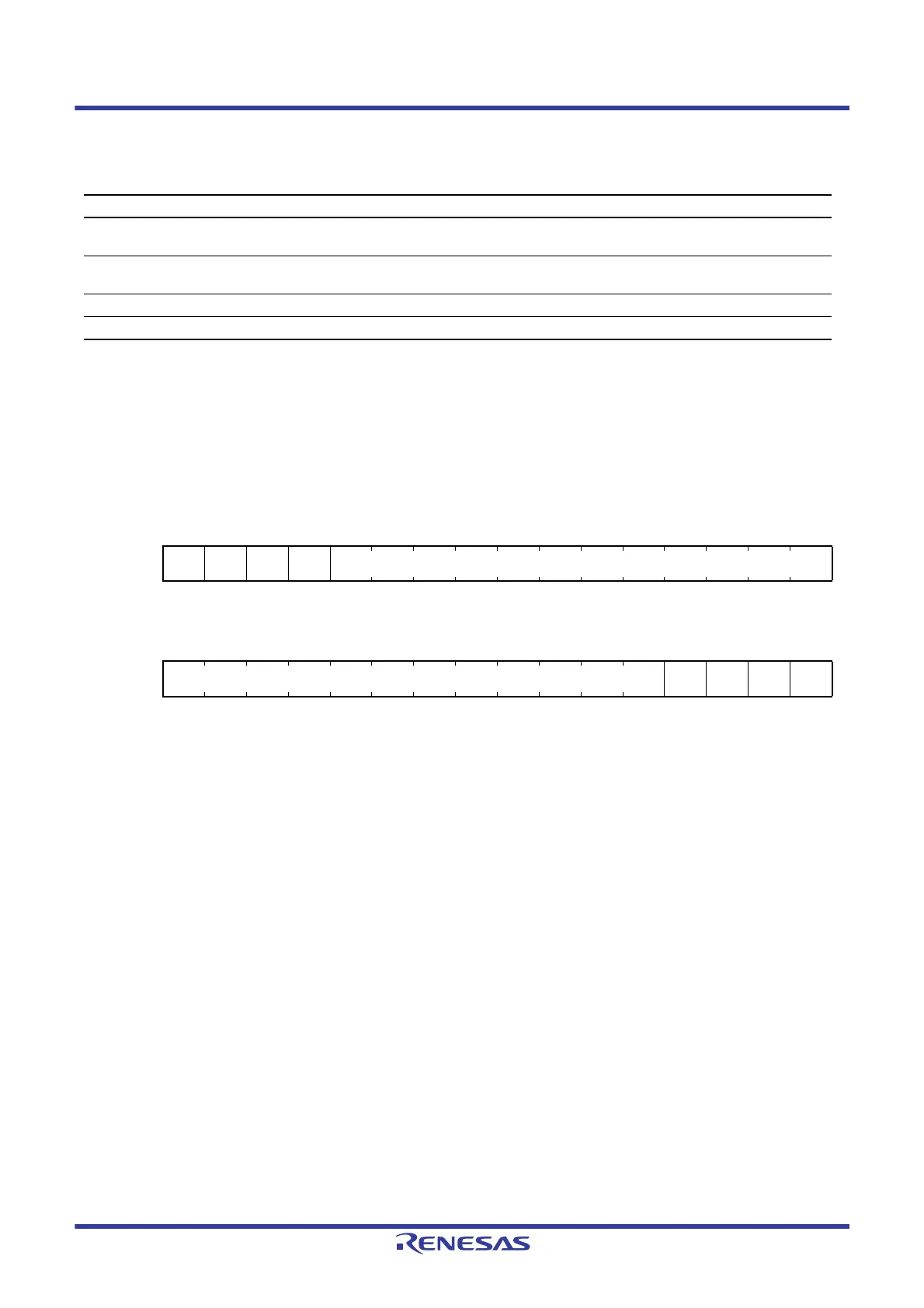
Address(es): DA.DADR0 0008 8040h, DA.DADR1 0008 8042h
DADPR.DPSEL bit = 0 (data is right-justified)
b15 b14 b13 b12 b11 b10 b9 b8 b7 b6 b5 b4 b3 b2 b1 b0
————
Value after reset:
0000000000000000
DADPR.DPSEL bit = 1 (data is left-justified)
b15 b14 b13 b12 b11 b10 b9 b8 b7 b6 b5 b4 b3 b2 b1 b0
————
Value after reset:
0000000000000000

 Loading...


