R01UH0823EJ0100 Rev.1.00 Page 418 of 1823
Jul 31, 2019
RX23W Group 20. Event Link Controller (ELC)
20.2.8 Port Group Control Register n (PGCn) (n = 1, 2)
x: Don’t care
For the port group set as an output, the PGCn register specifies the form of outputting the signal from the port when an
event signal is input. For the port group set as an input, the PGCn register enables/disables overwriting of the PDBFn
register and specifies the conditions of event generation (edge of the input signal).
Specify the I/O direction of the port by the corresponding bit in the PDR register.
Refer to
Table 20.4 for the PGCn register and corresponding ports.
Address(es): ELC.PGC1 0008 B125h, ELC.PGC2 0008 B126h
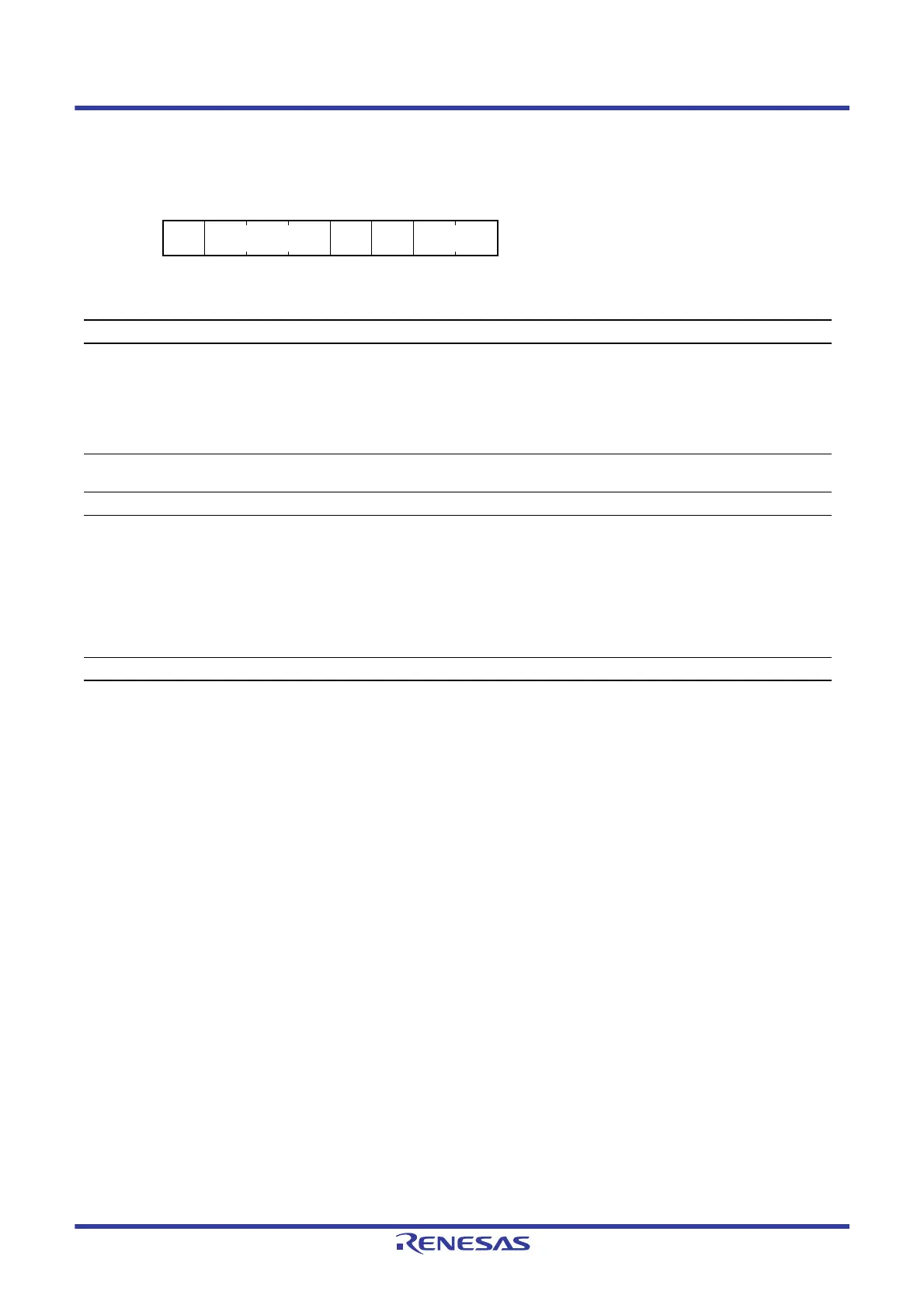
b7 b6 b5 b4 b3 b2 b1 b0
— PGCO[2:0] —
PGCO
VE
PGCI[1:0]
Value after reset:
10001000
Bit Symbol Bit Name Description R/W
b1, b0 PGCI[1:0] Event Output Edge Select
b1 b0
0 0: Event signal is output upon detection of the rising edge
of the input signal to the port.
0 1: Event signal is output upon detection of the falling edge
of the input signal to the port.
1 x: Event signal is output upon detection of both the rising
and falling edges of the input signal to the port.
R/W
b2 PGCOVE PDBF Overwrite 0: Overwriting the PDBFn register is disabled.
1: Overwriting the PDBFn register is enabled.
R/W
b3 — Reserved This bit is read as 1. The write value should be 1. R/W
b6 to b4 PGCO[2:0] Port Group Operation Select
b6 b4
0 0 0: Low is output when an event signal is input.
0 0 1: High is output when an event signal is input.
0 1 0: The output is toggled (inverted) when an event signal
is input.
0 1 1: The buffer value is output when an event signal is
input.
1 x x: The output data is rotated (from MSB to LSB) in the
port group when an event signal is input.
R/W
b7 — Reserved This bit is read as 1. The write value should be 1. R/W

 Loading...


