R01UH0823EJ0100 Rev.1.00 Page 1502 of 1823
Jul 31, 2019
RX23W Group 43. Capacitive Touch Sensing Unit (CTSU)
43.2.10 CTSU Channel Transmit/Receive Control Register 4 (CTSUCHTRC4)
Note 1. TS32, TS33, and TS34 pins are not available.
The CTSUCHTRC4 register should be set when the CTSUCR0.CTSUSTRT bit is 0.
CTSUCHTRC4j Bit (CTSU Channel Transmit/Receive Control 4j) (j = 0 to 3)
This bit allocates reception or transmission to the corresponding TS pin in full scan mode. The setting of this bit is
ignored in self-capacitance single scan mode and multi-scan mode.
CTSUCHTRC40 bit corresponds to TS32 pin and CTSUCHTRC43 bit corresponds to TS35 pin.
Note: TS32, TS33, and TS34 pins are not available.
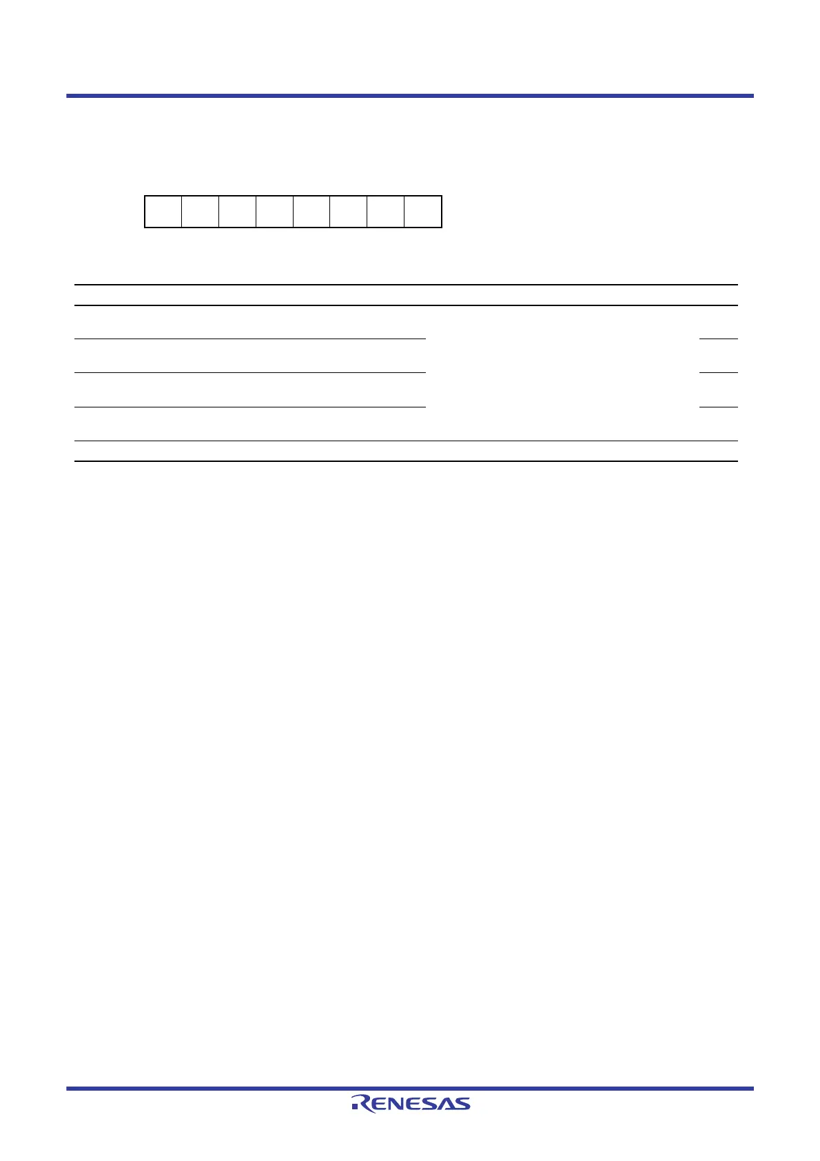
Address(es): CTSU.CTSUCHTRC4 000A 090Fh
b7 b6 b5 b4 b3 b2 b1 b0
————
CTSUC
HTRC43
CTSUC
HTRC42
CTSUC
HTRC41
CTSUC
HTRC40
Value after reset:
00000000
Bit Symbol Bit Name Description R/W
b0 CTSUCHTRC40 CTSU Channel Transmit/Receive
Control 40
0: Reception
1: Transmission
These bits specify the TS32 to TS35 pins*
1
.
R/W
b1 CTSUCHTRC41 CTSU Channel Transmit/Receive
Control 41
R/W
b2 CTSUCHTRC42 CTSU Channel Transmit/Receive
Control 42
R/W
b3 CTSUCHTRC43 CTSU Channel Transmit/Receive
Control 43
R/W
b7 to b4 — Reserved These bits are read as 0. The write value should be 0. R/W

 Loading...


