R01UH0823EJ0100 Rev.1.00 Page 1674 of 1823
Jul 31, 2019
RX23W Group 50. Flash Memory (FLASH)
50.4.15 Flash Write Buffer n Register (FWBn) (n = 0 to 3)
This register is used to set the data for programming the ROM, E2 DataFlash, or extra area. The data can be written in
ROM P/E mode or E2 DataFlash P/E mode.
This register is initialized by a reset or setting the FRESETR.FRESET bit to 1. Data cannot be written to this register
while the FRESETR.FRESET bit is 1.
The read value of this register is undefined while executing a software command set by the FCR register or the FEXCR
register.
When programming the extra area, set the 4-byte data for programming in registers FWB0 and FWB1.
When programming the ROM, set the 8-byte data for programming in registers FWB0 to FWB3.
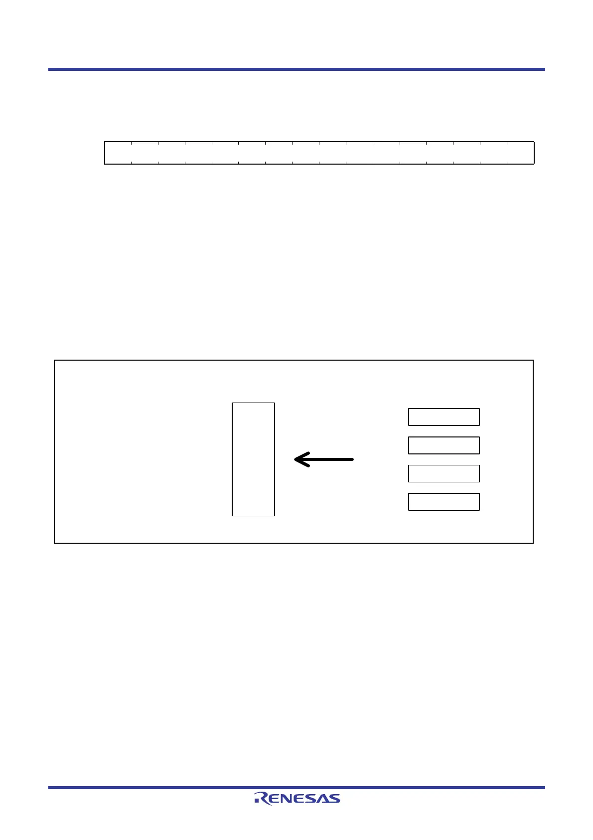
Figure 50.3 shows the
relationship between the addresses indicated by registers FSARH and FSARL and the data set in the FWBn register.
Figure 50.3 FWBn Register Setting Values and Data Allocation in the ROM
Address(es): FLASH.FWB0 007F C130h, FLASH.FWB1 007F C138h, FLASH.FWB2 007F C140h, FLASH.FWB3 007F C144h
b15 b14 b13 b12 b11 b10 b9 b8 b7 b6 b5 b4 b3 b2 b1 b0
Value after reset:
0000000000000000
When programming the E2 DataFlash, set the data for programming in the lower 8 bits in the FWB0 register.
ROM
01h
Address 1 23h
Address 2 45h
Address 3 67h
Address 4 89h
Address 5 ABh
Address 6 CDh
Address 7 EFh
Registers
FWB0
2301h
FWB1
6745h
FWB2
AB89h
FWB3
EFCDh
FSARH and FSARL + Address 0

 Loading...


