R01UH0823EJ0100 Rev.1.00 Page 481 of 1823
Jul 31, 2019
RX23W Group 23. Multi-Function Timer Pulse Unit 2 (MTU2a)
23.2.3 Timer I/O Control Register (TIOR)
MTU0.TIORH, MTU1.TIOR, MTU2.TIOR, MTU3.TIORH, MTU4.TIORH
Note 1. If the IOm[3:0] (m = A, B) bits are changed to an “output prohibited” setting (0000b or 0100b) while output of the low or high level
or toggling of the output in response to compare matches is in progress, the output becomes high-impedance.
MTU0.TIORL, MTU3.TIORL, MTU4.TIORL
Note 1. If the IOm[3:0] (m = C, D) bits are changed to an “output prohibited” setting (0000b or 0100b) while output of the low or high level
or toggling of the output in response to compare matches is in progress, the output becomes high-impedance.
Note 2. In MTU0, which have no MTIOC0D pin, this bit is reserved. It is read as 0. The write value should be 0.
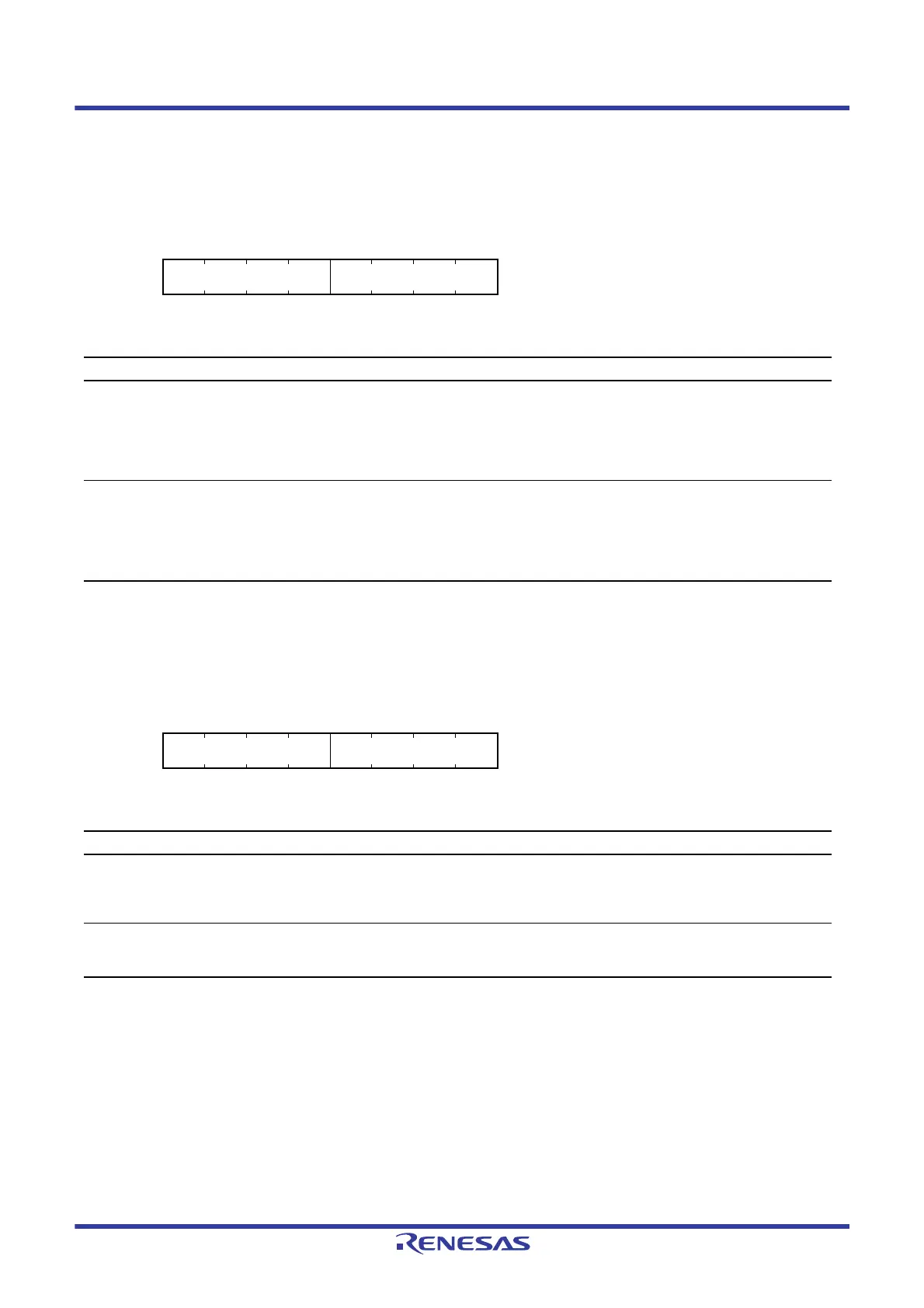
Address(es): MTU0.TIORH 000D 0B02h, MTU1.TIOR 000D 0B82h, MTU2.TIOR 000D 0C02h, MTU3.TIORH 000D 0A04h,
MTU4.TIORH 000D 0A06h
b7 b6 b5 b4 b3 b2 b1 b0
IOB[3:0] IOA[3:0]
Value after reset:
00000000
Bit Symbol Bit Name Description R/W
b3 to b0 IOA[3:0] I/O Control A Refer to the following tables.*
1
MTU0.TIORH: Table 23.18
MTU1.TIOR: Table 23.20
MTU2.TIOR: Table 23.21
MTU3.TIORH: Table 23.22
MTU4.TIORH: Table 23.24
R/W
b7 to b4 IOB[3:0] I/O Control B Refer to the following tables.*
1
MTU0.TIORH: Table 23.11
MTU1.TIOR: Table 23.12
MTU2.TIOR: Table 23.13
MTU3.TIORH: Table 23.14
MTU4.TIORH: Table 23.16
R/W
Address(es): MTU0.TIORL 000D 0B03h, MTU3.TIORL 000D 0A05h, MTU4.TIORL 000D 0A07h
b7 b6 b5 b4 b3 b2 b1 b0
IOD[3:0] IOC[3:0]
Value after reset:
00000000
Bit Symbol Bit Name Description R/W
b3 to b0 IOC[3:0] I/O Control C Refer to the following tables.*
1
MTU0.TIORL: Table 23.19
MTU3.TIORL: Table 23.23
MTU4.TIORL: Table 23.25
R/W
b7 to b4 IOD[3:0] I/O Control D*
2
Refer to the following tables.*
1
MTU3.TIORL: Table 23.15
MTU4.TIORL: Table 23.17
R/W

 Loading...


