R01UH0823EJ0100 Rev.1.00 Page 1555 of 1823
Jul 31, 2019
RX23W Group 44. 12-Bit A/D Converter (S12ADE)
44.2.14 A/D Sampling State Register n (ADSSTRn) (n = 0 to 7, L, T, O)
The ADSSTRn register sets the sampling time for analog input.
If one state is one ADCLK (A/D conversion clock) cycle and the ADCLK clock is 54 MHz, one state is 18.5 ns. The
initial value is 13 states. If the impedance of analog input signal source is too high to secure sufficient sampling time or if
the ADCLK clock is slow, the sampling time can be adjusted. The ADSSTRn register should be set while the
ADCSR.ADST bit is 0. The lower-limit value for sampling time differs depending on the PCLK to ADCLK frequency
ratio.
Set a value that is 5 states or more when PCLK to ADCLK frequency ratio = 1:1, 2:1, 4:1, or 8:1.
Set a value that is 6 states or more when PCLK to ADCLK frequency ratio = 1:2 or 1:4.
Table 44.8 shows the relationship between the A/D sampling state register and the relevant channels.
For details, refer to
section 44.3.6, Analog Input Sampling Time and Scan Conversion Time.
Note 1. When performing A/D conversion of the temperature sensor output or internal reference voltage, the sampling time should be 5
μs or longer. Since the maximum number of states that can be set by this register is 255, take note of the ADCLK frequency. For
example, when ADCLK = 54 MHz, the sampling time does not reach 5 μs even if 255 states is set.
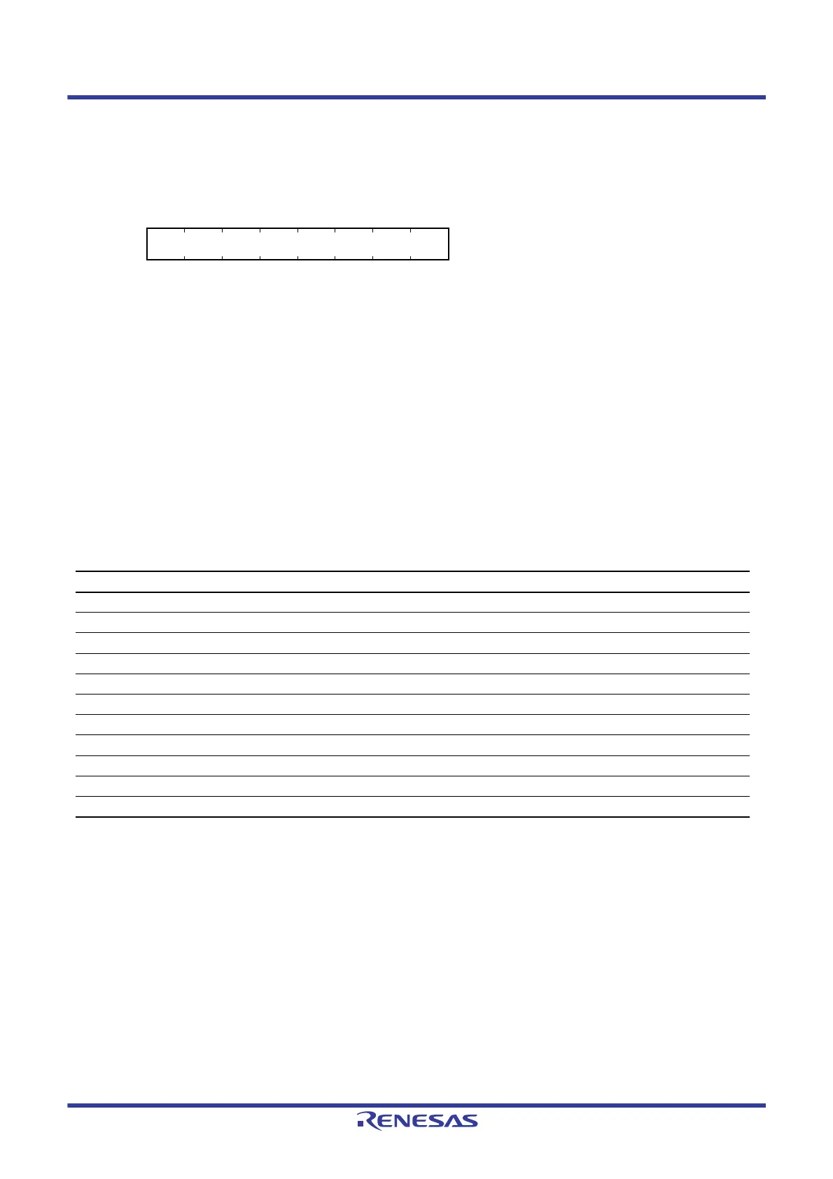
Address(es): S12AD.ADSSTRL 0008 90DDh, S12AD.ADSSTRT 0008 90DEh, S12AD.ADSSTRO 0008 90DFh,
S12AD.ADSSTR0 0008 90E0h, S12AD.ADSSTR1 0008 90E1h, S12AD.ADSSTR2 0008 90E2h,
S12AD.ADSSTR3 0008 90E3h, S12AD.ADSSTR4 0008 90E4h, S12AD.ADSSTR5 0008 90E5h,
S12AD.ADSSTR6 0008 90E6h, S12AD.ADSSTR7 0008 90E7h
b7 b6 b5 b4 b3 b2 b1 b0
Value after reset:
00001101
Table 44.8 Relationship between A/D Sampling State Register and Relevant Channels
Register Name Channels
ADSSTR0 AN000
ADSSTR1 AN001
ADSSTR2 AN002
ADSSTR3 AN003
ADSSTR4 AN004
ADSSTR5 AN005
ADSSTR6 AN006
ADSSTR7 AN007
ADSSTRL AN016 to AN020, AN027
ADSSTRT Temperature sensor output*
1
ADSSTRO Internal reference voltage*
1

 Loading...


