R01UH0823EJ0100 Rev.1.00 Page 350 of 1823
Jul 31, 2019
RX23W Group 18. DMA Controller (DMACA)
18.2.8 DMA Offset Register (DMOFR)
Write to this register while the DMAC operation is stopped or DMA transfer is disabled (not during data transfer).
Setting bits 31 to 25 is invalid; a value of bit 24 is extended to bits 31 to 25. Reading DMOFR returns the extended value.
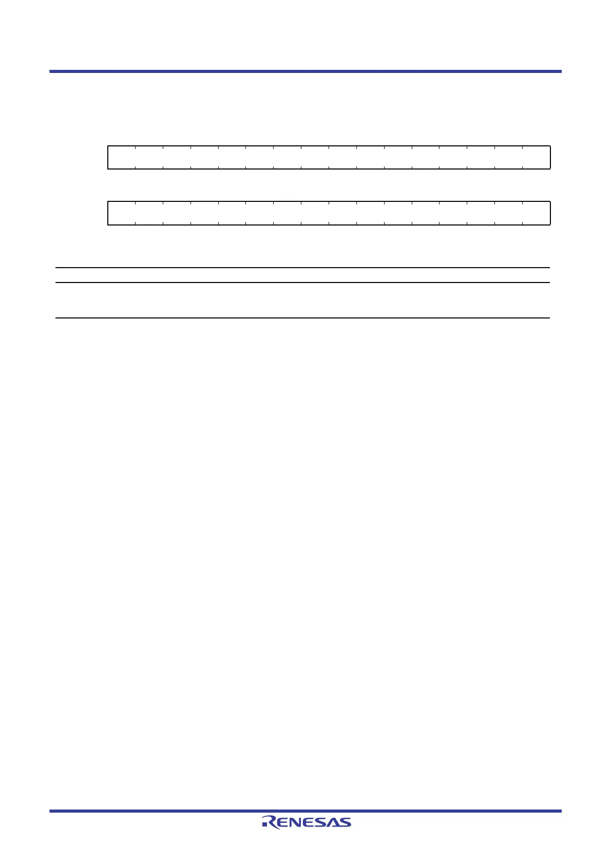
Address(es): DMAC0.DMOFR 0008 2018h
b31 b30 b29 b28 b27 b26 b25 b24 b23 b22 b21 b20 b19 b18 b17 b16
Value after reset:
0000000000000000
b15 b14 b13 b12 b11 b10 b9 b8 b7 b6 b5 b4 b3 b2 b1 b0
Value after reset:
0000000000000000
Bit Description Setting Range R/W
b31 to b0 Specifies the offset when offset addition is selected
as the address update mode for transfer source or
destination.
0000 0000h to 00FF FFFFh (0 bytes to (16 M – 1) bytes)
FF00 0000h to FFFF FFFFh (–16 Mbytes to –1 byte)
R/W

 Loading...


