R01UH0823EJ0100 Rev.1.00 Page 1573 of 1823
Jul 31, 2019
RX23W Group 44. 12-Bit A/D Converter (S12ADE)
44.2.30 A/D High-Potential/Low-Potential Reference Voltage Control Register
(ADHVREFCNT)
The ADHVREFCNT register specifies the high-potential and low-potential reference voltages. Set this register before
performing A/D conversion.
HVSEL[1:0] Bits (High-Potential Reference Voltage Select)
These bits are used to set the high-potential reference voltage. AVCC0 or VREFH0 is selectable as the high-potential
reference voltage.
LVSEL Bit (Low-Potential Reference Voltage Select)
This bit is used to set the low-potential reference voltage. AVSS0 or VREFL0 is selectable as the low-potential reference
voltage.
ADSLP Bit (Sleep)
This bit is used to transition the 12-bit A/D converter to the standby state. Set the ADSLP bit to 1 only when modifying
the ADCSR.ADHSC bit. In other cases, setting the ADSLP bit to 1 is prohibited.
After the ADSLP bit is set to 1, wait at least 5 μs before clearing this bit to 0. Furthermore, after the ADSLP bit is cleared
to 0, wait at least 1 μs and then start the A/D conversion.
For the ADHSC bit rewriting procedure, see
section 44.8.10, ADHSC Bit Rewriting Procedure.
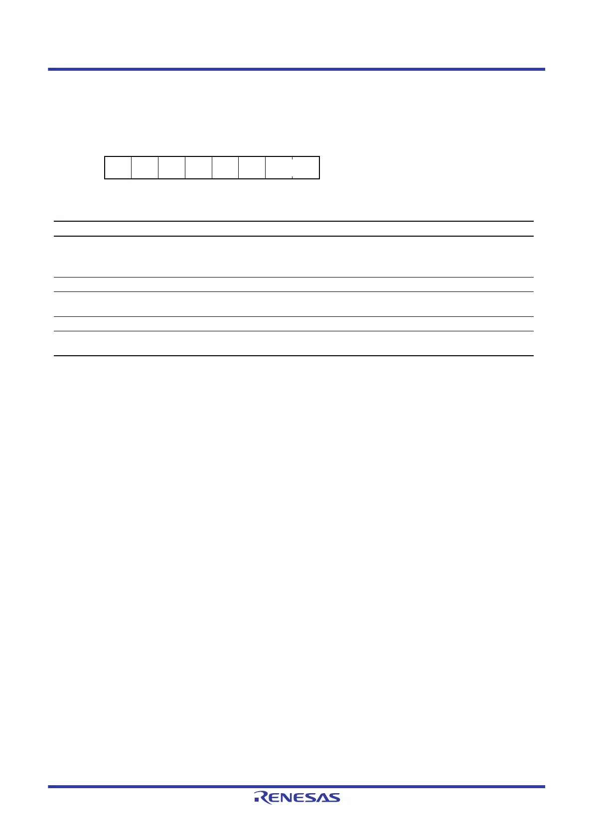
Address(es): S12AD.ADHVREFCNT 0008 908Ah
b7 b6 b5 b4 b3 b2 b1 b0
ADSLP
——
LVSEL
——
HVSEL[1:0]
Value after reset:
0
0000000
Bit Symbol Bit Name Description R/W
b1, b0 HVSEL[1:0] High-Potential Reference
Voltage Select
b1 b0
0 0: AVCC0 is selected as the high-potential reference voltage.
0 1: VREFH0 is selected as the high-potential reference voltage.
Settings other than above are prohibited.
R/W
b3, b2 — Reserved These bits are read as 0. The write value should be 0. R/W
b4 LVSEL Low-Potential Reference
Voltage Select
0: AVSS0 is selected as the low-potential reference voltage.
1: VREFL0 is selected as the low-potential reference voltage.
R/W
b6, b5 — Reserved These bits are read as 0. The write value should be 0. R/W
b7 ADSLP Sleep 0: Normal operation
1: Standby state
R/W

 Loading...


