R01UH0823EJ0100 Rev.1.00 Page 736 of 1823
Jul 31, 2019
RX23W Group 26. 8-Bit Timer (TMR)
26.2.6 Timer Control/Status Register (TCSR)
TMR0.TCSR, TMR2.TCSR
Note 1. When all OSA[1:0] and OSB[1:0] bits are 0, the output enable signal corresponding to the TMOn pin is negated and a request
for high-impedance output is issued to the I/O port. Timer output pin is driven low until the first compare-match occurs after a
reset when at least one of the OSA[1:0] and OSB[1:0] bits is 1.
OSA[1:0] Bits (Output Select A)
These bits select a method of TMOn pin output when compare match A of TCORA and TCNT occurs.
OSB[1:0] Bits (Output Select B)
These bits select a method of TMOn pin output when compare match B of TCORB and TCNT occurs.
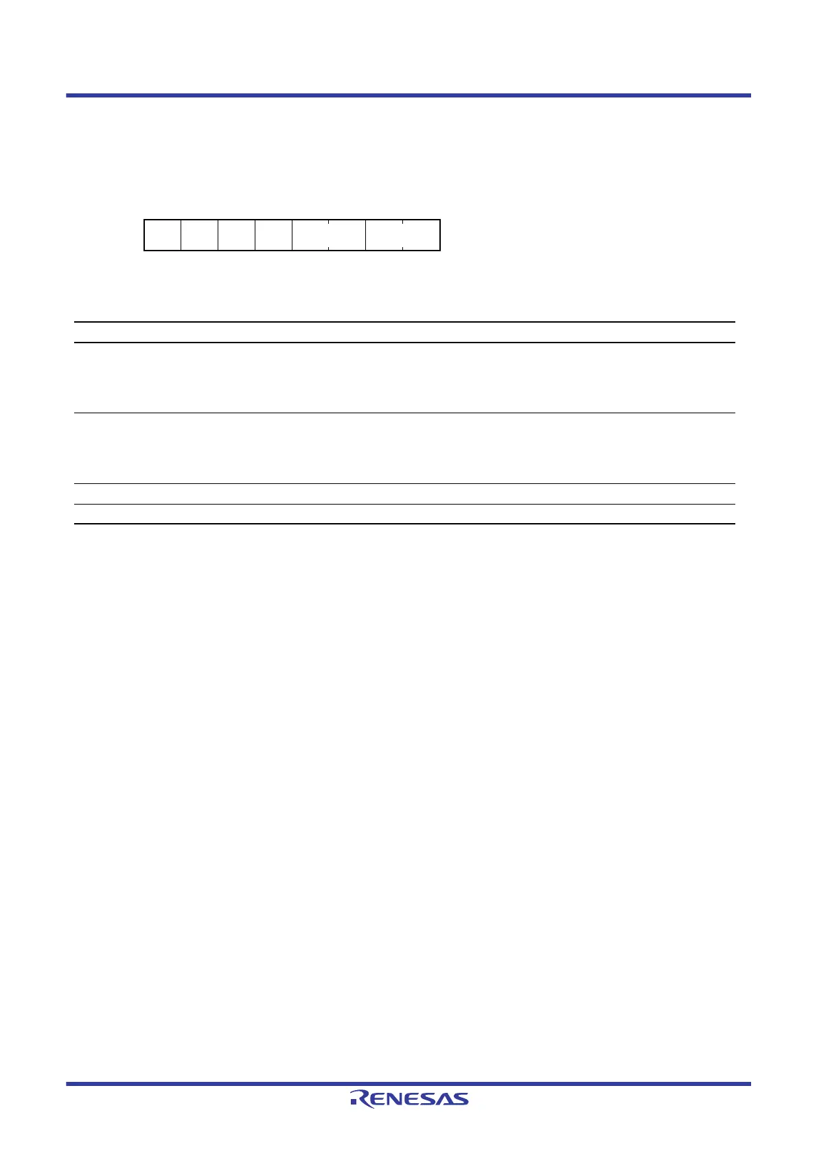
Address(es): TMR0.TCSR 0008 8202h, TMR2.TCSR 0008 8212h
b7 b6 b5 b4 b3 b2 b1 b0
———— OSB[1:0] OSA[1:0]
Value after reset:
xxx00000
x: Undefined
Bit Symbol Bit Name Description R/W
b1, b0 OSA[1:0] Output Select A*
1
b1 b0
0 0: No change
0 1: Low is output
1 0: High is output
1 1: Output is inverted (toggle output)
R/W
b3, b2 OSB[1:0] Output Select B*
1
b3 b2
0 0: No change
0 1: Low is output
1 0: High is output
1 1: Output is inverted (toggle output)
R/W
b4 — Reserved This bit is read as 0. The write value should be 0. R/W
b7 to b5 — Reserved These bits are read as an undefined value. The write value should be 1. R/W

 Loading...


