R01UH0823EJ0100 Rev.1.00 Page 1146 of 1823
Jul 31, 2019
RX23W Group 35. I
2
C-bus Interface (RIICa)
35.3.2 Initial Settings
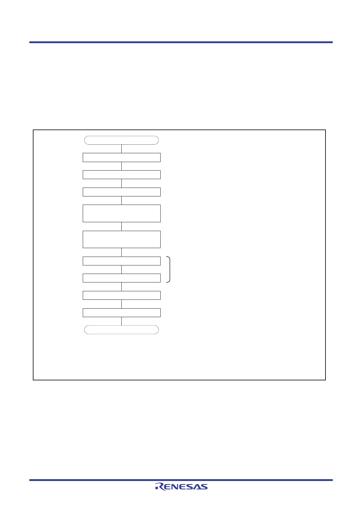
Before starting data transmission and reception, initialize the RIIC according to the procedure in Figure 35.5.
Set the ICCR1.ICE bit to 1 (internal reset) after setting the ICCR1.IICRST bit to 1 (RIIC reset) with the ICCR1.ICE bit
set to 0 (SCL0 and SDA0 pins in inactive state). This initializes the various flags and internal state of the ICSR1 register.
After that, set registers SARLy, SARUy, ICSER, ICMR1, ICBRH, and ICBRL (y = 0 to 2), and set the other registers as
necessary (for initial settings of the RIIC, see
Figure 35.5). When the necessary register settings have been completed,
set the ICCR1.IICRST bit to 0 (releases the RIIC reset). This step is not necessary if initialization of the RIIC has already
been completed.
Figure 35.5 Example of RIIC Initialization Flowchart
Set transfer bit rate*
1
*
2
Initial settings
Set ICMR1.CKS[2:0] bits and
ICBRL/ICBRH registers
Set registers ICMR2 and ICMR3
Set ICFER register
Set ICCR1.ICE bit to 0
Set ICCR1.IICRST bit to 1
Set ICCR1.ICE bit to 1
RIIC reset
Set registers SARLy and SARUy.
Set ICSER register
Set slave address format and slave address
Release from the internal reset state
Set interrupt enable
y = 0 to 2
Set ICIER register
Set ICCR1.IICRST bit to 0
End
Note 1. When the RIIC is used only in slave mode, set the ICBRL register to a value
longer than the data setup time.
Note 2. Set these registers as necessary.
SCL0 and SDA0 pins not driven
Internal reset, SCL0 and SDA0 pins in active state

 Loading...


