R01UH0823EJ0100 Rev.1.00 Page 755 of 1823
Jul 31, 2019
RX23W Group 27. Compare Match Timer (CMT)
27.2 Register Descriptions
27.2.1 Compare Match Timer Start Register 0 (CMSTR0)
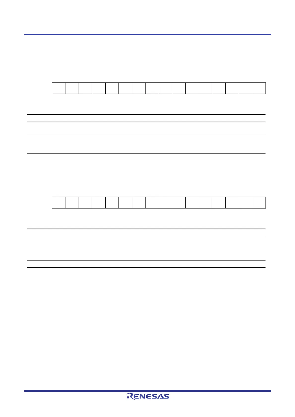
27.2.2 Compare Match Timer Start Register 1 (CMSTR1)
Address(es): 0008 8000h
b15 b14 b13 b12 b11 b10 b9 b8 b7 b6 b5 b4 b3 b2 b1 b0
——————————————STR1STR0
Value after reset:
0000000000000000
Bit Symbol Bit Name Description R/W
b0 STR0 Count Start 0 0: CMT0.CMCNT count is stopped.
1: CMT0.CMCNT count is started.
R/W
b1 STR1 Count Start 1 0: CMT1.CMCNT count is stopped.
1: CMT1.CMCNT count is started.
R/W
b15 to b2 — Reserved These bits are read as 0. The write value should be 0. R/W
Address(es): 0008 8010h
b15 b14 b13 b12 b11 b10 b9 b8 b7 b6 b5 b4 b3 b2 b1 b0
——————————————STR3STR2
Value after reset:
0000000000000000
Bit Symbol Bit Name Description R/W
b0 STR2 Count Start 2 0: CMT2.CMCNT count is stopped.
1: CMT2.CMCNT count is started.
R/W
b1 STR3 Count Start 3 0: CMT3.CMCNT count is stopped.
1: CMT3.CMCNT count is started.
R/W
b15 to b2 — Reserved These bits are read as 0. The write value should be 0. R/W

 Loading...


