R01UH0823EJ0100 Rev.1.00 Page 257 of 1823
Jul 31, 2019
RX23W Group 13. Register Write Protection Function
13.1 Register Descriptions
13.1.1 Protect Register (PRCR)
Note 1. Write data is not retained.
PRCi Bits (Protect Bit i) (i = 0 to 3)
These bits enable or disable writing to the corresponding registers to be protected.
Setting the PRCi bits to 1 and 0 enable and disable writing to the corresponding registers to be protected, respectively.
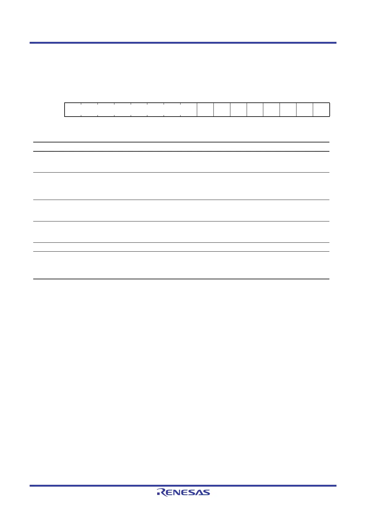
Address(es): 0008 03FEh
b15 b14 b13 b12 b11 b10 b9 b8 b7 b6 b5 b4 b3 b2 b1 b0
PRKEY[7:0] ————PRC3PRC2PRC1PRC0
Value after reset:
0000000000000000
Bit Symbol Bit Name Function R/W
b0 PRC0 Protect Bit 0 Enables writing to the registers related to the clock generation circuit.
0: Write disabled
1: Write enabled
R/W
b1 PRC1 Protect Bit 1 Enables writing to the registers related to operating modes, low power
consumption functions, the clock generation circuit, and software reset.
0: Write disabled
1: Write enabled
R/W
b2 PRC2 Protect Bit 2 Enables writing to the registers related to the low power timer.
0: Write disabled
1: Write enabled
R/W
b3 PRC3 Protect Bit 3 Enables writing to the registers related to the LVD.
0: Write disabled
1: Write enabled
R/W
b7 to b4 — Reserved These bits are read as 0. The write value should be 0. R/W
b15 to b8 PRKEY[7:0] PRC Key Code These bits control permission and prohibition of writing to the PRCR
register.
To modify the PRCR register, write A5h to the 8 higher-order bits and the
desired value to the 8 lower-order bits as a 16-bit unit.
R/W*
1
 Loading...


