R01UH0823EJ0100 Rev.1.00 Page 164 of 1823
Jul 31, 2019
RX23W Group 8. Voltage Detection Circuit (LVDAb)
8.4 Reset from Voltage Monitor 0
When using the reset from voltage monitor 0, clear the voltage detection 0 circuit start bit (OFS1.LVDAS) to 0 (enabling
the voltage monitor 0 reset after a reset).
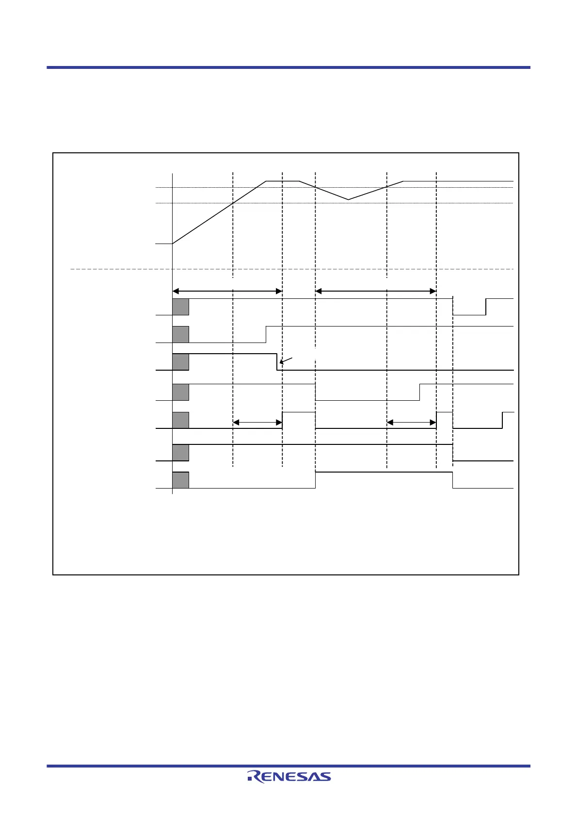
Figure 8.3 shows an example of operations for a voltage monitoring 0 reset.
Figure 8.3 Example of Voltage Monitoring 0 Reset Operation
External voltage VCC
VPOR*
1
RES# pin
POR detection signal
(Low is valid)
Internal reset signal
tPOR*
2
tLVD0*
2
RES# pin reset
RSTSR0.PORF
Voltage detection 0
signal (Low is valid)
RSTSR0.LVD0RF
Vdet0*
1
LVD0 enable/disable
signal (Low is valid)
*
3
Power-on reset state Voltage monitoring 0 reset state
Set by OFS1.LVDAS
VCC
0
VCC
0
VCC
0
VCC
0
VCC
0
VCC
0
VCC
0
Note: For details on the electrical characteristics, see the Electrical Characteristics section.
Note 1. Vdet0 indicates the detection level for a voltage monitoring 0 reset and VPOR indicates the detection level for a
power-on reset.
Note 2. tPOR indicates the period of a power-on reset and tLVD0 indicates the period of a voltage monitoring 0 reset.
Note 3. At the time the power-supply voltage rises, VCC must rise to at least the minimum guaranteed voltage before release
from the POR reset state.

 Loading...


