R01UH0823EJ0100 Rev.1.00 Page 450 of 1823
Jul 31, 2019
RX23W Group 21. I/O Ports
21.5 Handling of Unused Pins
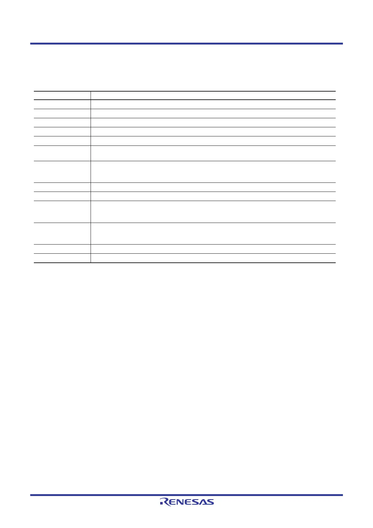
The configuration of unused pins is listed in Table 21.5.
Note 1. Clear the PORTn.PMR bit, the PmnPFS.ISEL bit and the PmnPFS.ASEL bit to 0.
Note 2. In the case of release when the setting is for output, the port is an input over the period from release from the reset state to the
pin becoming an output. Since the voltage on the pin is undefined while it is an input, this may lead to an increase in the current
drawn.
Table 21.5 Unused Pin Configuration
Pin Name Description
VBATT Connect this pin to VCC.
MD (Always used as mode pins)
RES# Connect this pin to VCC via a pull-up resistor.
P35/NMI Connect this pin to VCC via a pull-up resistor.
USB0_DM, USB0_DP Leave this pin open.
P36/EXTAL When the main clock is not used, set the MOSCCR.MOSTP bit to 1 (general port P36).
When this pin is not used as port P36 either, it is configured in the same way as port 1 to 3, B to E, J.
P37/XTAL When the main clock is not used, set the MOSCCR.MOSTP bit to 1 (general port P37).
When this pin is not used as port P37 either, it is configured in the same way as port 1 to 3, B to E, J.
When the external clock is input to the EXTAL pin, leave this pin open.
XCIN Connect this pin to VSS via a pull-down resistor.
XCOUT Leave this pin open.
Ports 1 to 3,
Ports B to E, J
If the direction setting is for input (PORTn.PDR = 0), the corresponding pin is connected to VCC (pulled up)
via a resistor or to VSS (pulled down) via a resistor.*
1
If the direction setting is for output (PORTn.PDR = 1), the pin is released.*
1
, *
2
Ports 0, 4 If the direction setting is for input (PORTn.PDR = 0), the corresponding pin is connected to AVCC0 (pulled
up) via a resistor or to AVSS0 (pulled down) via a resistor.*
1
If the direction setting is for output (PORTn.PDR = 1), the pin is released.*
1
, *
2
VREFH0 Connect this pin to AVCC0.
VREFL0 Connect this pin to AVSS0.

 Loading...


