R01UH0823EJ0100 Rev.1.00 Page 158 of 1823
Jul 31, 2019
RX23W Group 8. Voltage Detection Circuit (LVDAb)
8.2 Register Descriptions
8.2.1 Voltage Monitoring 1 Circuit Control Register 1 (LVD1CR1)
Note: Set the PRCR.PRC3 bit to 1 (write enabled) before rewriting this register.
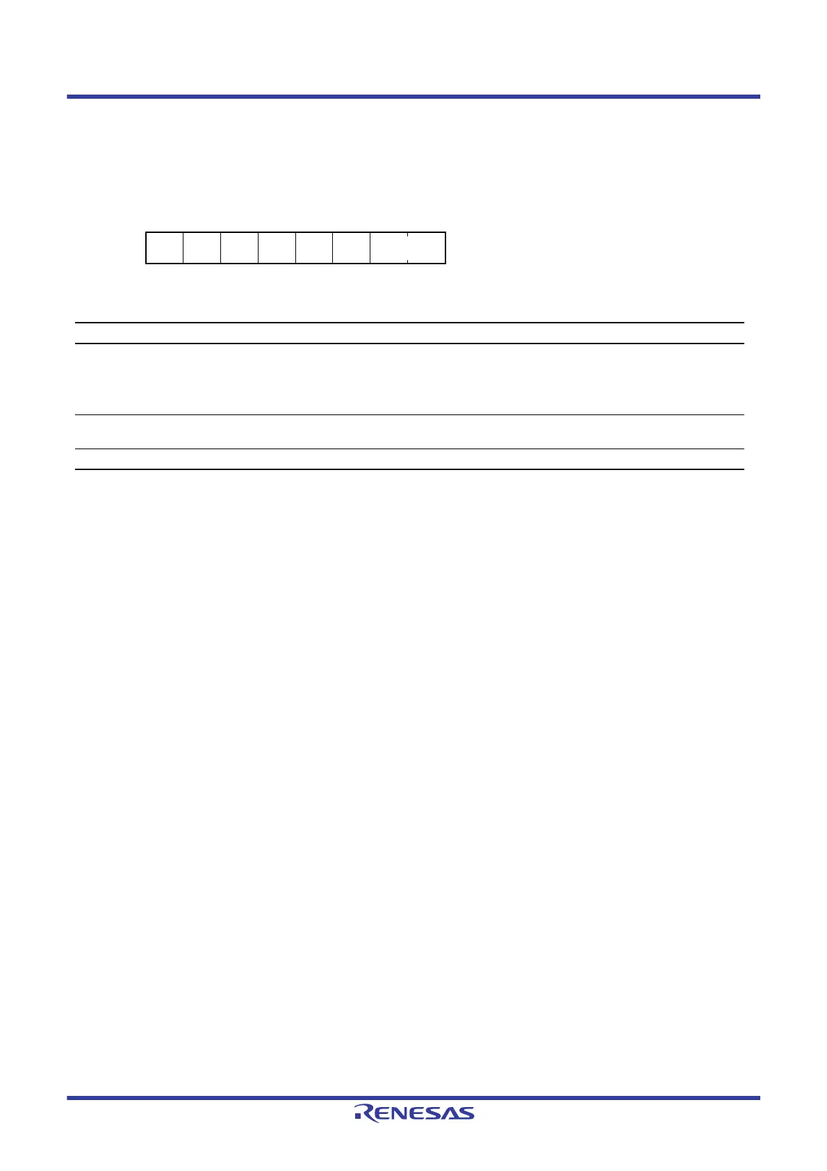
Address(es): 0008 00E0h
b7 b6 b5 b4 b3 b2 b1 b0
—————
LVD1IR
QSEL
LVD1IDTSEL[1:
0]
Value after reset:
00000001
Bit Symbol Bit Name Description R/W
b1, b0 LVD1IDTSEL
[1:0]
Voltage Monitoring 1 Interrupt
ELC Event Generation Condition Select
b1 b0
0 0: When VCC Vdet1 (rise) is detected
0 1: When VCC < Vdet1 (drop) is detected
1 0: When drop and rise are detected
1 1: Setting prohibited
R/W
b2 LVD1IRQSEL Voltage Monitoring 1 Interrupt Type Select 0: Non-maskable interrupt
1: Maskable interrupt
R/W
b7 to b3 — Reserved These bits are read as 0. The write value should be 0. R/W

 Loading...


