R01UH0823EJ0100 Rev.1.00 Page 157 of 1823
Jul 31, 2019
RX23W Group 8. Voltage Detection Circuit (LVDAb)
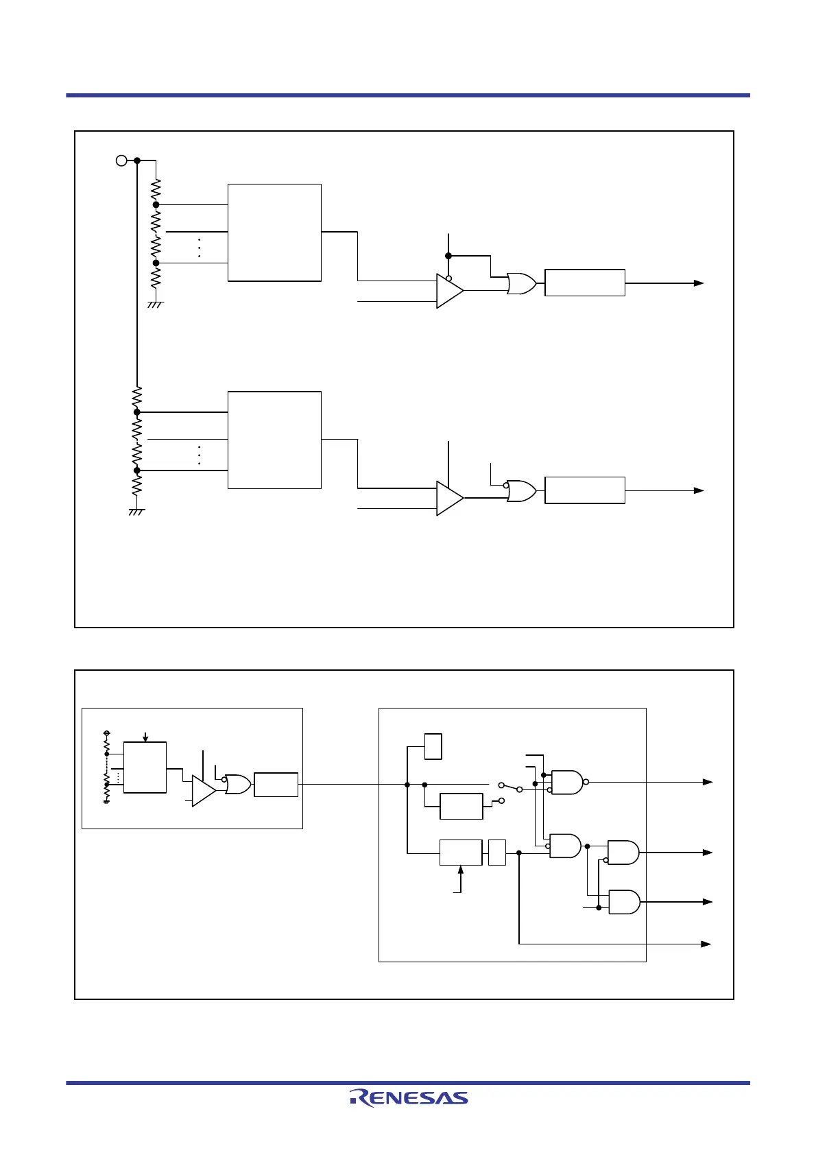
Figure 8.1 Block Diagram of the LVD
Figure 8.2 Block Diagram of Voltage Monitoring 1 Interrupt/Reset Circuit
LVD1E
+
-
Vdet1
LVD1E: Bit in LVCMPCR
LVD1CMPE: Bit in LVD1CR0
LVD1LVL[3:0]: Bits in LVDLVLR
LVDAS,VDSEL[1:0]: Bits in OFS1
Voltage detection 1
signal
Internal reference voltage
(for detecting Vdet1)
Level selection
circuit
(10 levels)
LVD1CMPE
Analog noise
filter
LVDAS
+
-
VCC
Vdet0
Voltage detection 0
reset signal
Internal reference voltage
(for detecting Vdet0)
Level selection
circuit
(3 levels)
VDSEL[1:0]
Analog noise
filter
LVD1LVL[3:0]
Voltage detection 1 circuit
Voltage detection 1 signal will be high
when the LVD1E bit is 0 (disabled)
The setting of the LVD1DET bit will be 0
if 0 (undetected) is written in the program.
Voltage monitoring 1 interrupt/reset circuit
LVD1E: Bit in LVCMPCR
LVD1LVL[3:0]: Bits in LVDLVLR
LVD1CMPE, LVD1RIE, LVD1RI, LVD1RN: Bits in LVD1CR0
LVD1IDTSEL[1:0], LVD1IRQSEL: Bits in LVD1CR1
LVD1DET: Bit in LVD1SR
+
-
VCC
Internal reference
voltage
(for detection of Vdet1)
LVD1LVL[3:0]
LVD1CMPE
Level
selection
circuit
(14 levels)
LVD1DET
LVD1IRQSEL
Voltage monitoring 1
maskable interrupt
signal
Edge
selection
circuit
LVD1IDTSEL[1:0]
Fixed
period
negation
LVD1RN = 0
LVD1RN = 1
LVD1RI
LVD1RIE
b1
LVD1SR register
LVD1MON bit
Voltage monitoring 1
non-maskable
interrupt signal
Voltage monitoring 1
reset signal
(low is valid)
LVD1E
Voltage detection 1
signal
Analog
noise filter
Voltage detection 1
ELC event output
signal
 Loading...


