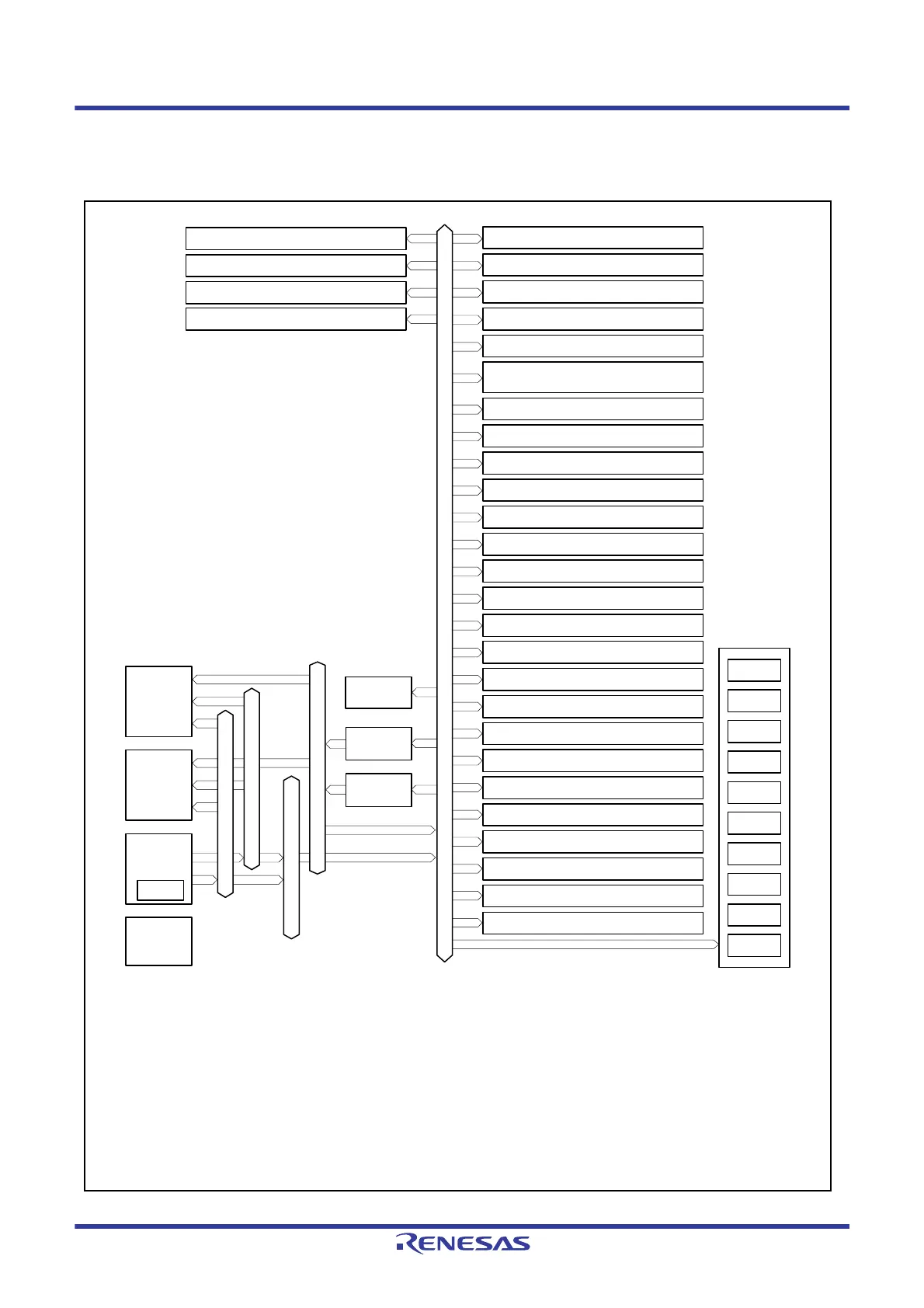
ICUb: Interrupt controller
DTCa: Data transfer controller
DMACA: DMA controller
WDTA: Watchdog timer
IWDTa: Independent watchdog timer
ELC: Event link controller
CRC: CRC (cyclic redundancy check) calculator
SCIg/SCIh: Serial communications interface
RSPIa: Serial peripheral interface
RIIC: I
2
C bus interface
SSI: Serial sound interface
TPUa: 16-bit timer pulse unit
MTU2a: Multi-function timer pulse unit 2
POE2a: Port output enable 2
TMR: 8-bit timer
CMT: Compare match timer
RTCe: Realtime clock
DOC: Data operation circuit
CAC: Clock frequency accuracy measurement circuit
BLE: Bluetooth Low Energy
SDHIa: SD host interface
RSCAN: CAN module
CTSU: Capacitive touch sensing unit
LPT: Low power timer
MPU: Memory protection unit
12-bit D/A converter × 2 channels
RIICa × 1 channel
DOC
RTCe
MTU2a × 5 channels
12-bit A/D converter × 14 channels
CMT × 2 channels (unit 0)
RSPIa × 1 channel
CAC
SCIh × 1 channel
POE2a
USB 2.0 host/function module
Temperature sensor
Comparator B × 2 channels
TMR × 2 channels (unit 0)
TMR × 2 channels (unit 1)
SSI
CMT × 2 channels (unit 1)
TPUa × 6 channels
BLE
E2 DataFlash
CRC
ELC
IWDTa
WDTA
SDHIa
RSCAN
CTSU
LPT
Clock
generation
circuit
RX CPU
RAM
ROM
Port 0
Port 1
Port 3
Port 4
SCIg × 3 channels
(including IrDA × 1 channel)
DTCa
ICUb
Port B
Port C
Port 2
Port D
Port E
DMACA
× 4 channels
MPU
Operand bus
Instruction bus
Internal main bus 1
Internal main bus 2
Internal peripheral buses 1 to 6
Port J

 Loading...


