R01UH0823EJ0100 Rev.1.00 Page 504 of 1823
Jul 31, 2019
RX23W Group 23. Multi-Function Timer Pulse Unit 2 (MTU2a)
23.2.17 Timer Output Control Registers 1 (TOCR1)
Note 1. Setting the TOCR1.TOCL bit to 1 prevents accidental modification when the CPU goes out of control.
Note 2. Setting the TOCR1.TOCS bit to 0 makes this bit setting valid.
Note 3. If dead-time is not generated, the negative-phase output is always the exact inverse of the positive-phase output. In this case,
only the OLSP bit is valid.
Note 4. This bit can be set to 1 only once after a power-on reset. After 1 is written, 0 cannot be written to the bit.
The TOCR1 registers enable or disable PWM-synchronized toggle output in complementary PWM mode and reset-
synchronized PWM mode, and control inversion of PWM output level.
OLSP Bit (Output Level Select P)
This bit selects the positive-phase output level in reset-synchronized PWM mode and complementary PWM mode.
OLSN Bit (Output Level Select N)
This bit selects the negative-phase output level in reset-synchronized PWM mode and complementary PWM mode.
TOCS Bit (TOC Select)
This bit selects either the TOCR1 or TOCR2 register setting to be used for the output level in complementary PWM
mode and reset-synchronized PWM mode.
TOCL Bit (TOC Register Write Protection)
This bit enables or disables write access to the TOCS, OLSN, and OLSP bits in the TOCR1 register.
PSYE Bit (PWM Synchronous Output Enable)
This bit enables or disables toggle output synchronized with the PWM cycle.
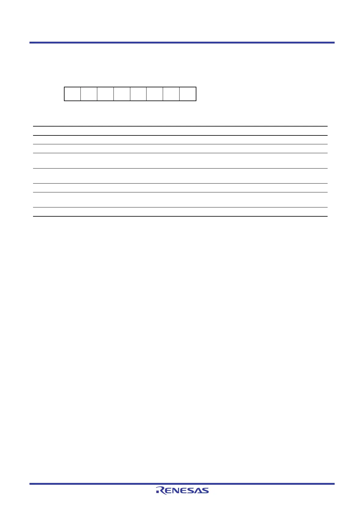
Address(es): MTU.TOCR1 000D 0A0Eh
b7 b6 b5 b4 b3 b2 b1 b0
— PSYE — — TOCL TOCS OLSN OLSP
Value after reset:
00000000
Bit Symbol Bit Name Description R/W
b0 OLSP Output Level Select P Refer to Table 23.27. R/W
b1 OLSN Output Level Select N Refer to Table 23.28. R/W
b2 TOCS TOC Select 0: TOCR1 setting is selected
1: TOCR2 setting is selected
R/W
b3 TOCL TOC Register Write Protection 0: Write access to the TOCS, OLSN, and OLSP bits is enabled
1: Write access to the TOCS, OLSN, and OLSP bits is disabled
R/W*
4
b5, b4 — Reserved These bits are read as 0. The write value should be 0. R/W
b6 PSYE PWM Synchronous Output
Enable
0: Toggle output is disabled
1: Toggle output is enabled
R/W
b7 — Reserved This bit is read as 0. The write value should be 0. R/W

 Loading...


