R01UH0823EJ0100 Rev.1.00 Page 1805 of 1823
Jul 31, 2019
RX23W Group 51. Electrical Characteristics
51.9 CTSU Characteristics
51.10 Characteristics of Power-On Reset Circuit and Voltage Detection Circuit
Note: These characteristics apply when noise is not superimposed on the power supply.
Note 1. n in the symbol Vdet0_n denotes the value of the OFS1.VDSEL[1:0] bits.
Note 2. n in the symbol Vdet1_n denotes the value of the LVDLVLR.LVD1LVL[3:0] bits.
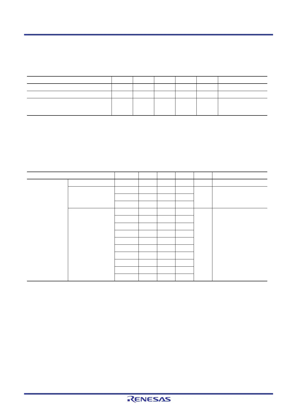
Table 51.50 CTSU Characteristics
Conditions: 1.8 V ≤ VCC = VCC_USB = AVCC0 = VCC_RF = AVCC_RF ≤ 3.6 V, VSS = AVSS0 = VSS_USB = VSS_RF = 0 V,
T
a
= –40 to +85°C
Item Symbol Min. Typ. Max. Unit Test Conditions
External capacitance connected to TSCAP pin C
tscap
91011nF
TS pin capacitive load C
base
— — 50 pF
Permissible output high current
I
OH
— — –24 mA When the mutual
capacitance method is
applied
Table 51.51 Characteristics of Power-On Reset Circuit and Voltage Detection Circuit (1)
Conditions: 1.8 V ≤ VCC = VCC_USB = AVCC0 = VCC_RF = AVCC_RF ≤ 3.6 V, VSS = AVSS0 = VSS_USB = VSS_RF = 0 V,
T
a
= –40 to +85°C
Item Symbol Min. Typ. Max. Unit Test Conditions
Voltage detection
level
Power-on reset (POR) V
POR
1.35 1.50 1.65 V Figure 51.63, Figure 51.64
Voltage detection circuit
(LVD0)*
1
V
det0_1
2.70 2.82 3.00 V Figure 51.65
At falling edge VCC
V
det0_2
2.37 2.51 2.67
V
det0_3
1.80 1.90 1.99
Voltage detection circuit
(LVD1)*
2
V
det1_4
2.99 3.10 3.29 V Figure 51.66
At falling edge VCC
V
det1_5
2.89 3.00 3.19
V
det1_6
2.79 2.90 3.09
V
det1_7
2.68 2.79 2.98
V
det1_8
2.57 2.68 2.87
V
det1_9
2.47 2.58 2.67
V
det1_A
2.37 2.48 2.57
V
det1_B
2.10 2.20 2.30
V
det1_C
1.86 1.96 2.06
V
det1_D
1.80 1.86 1.96

 Loading...


