R01UH0823EJ0100 Rev.1.00 Page 419 of 1823
Jul 31, 2019
RX23W Group 20. Event Link Controller (ELC)
20.2.9 Port Buffer Register n (PDBFn) (n = 1, 2)
The PDBFn register is an 8-bit readable/writable register used in combination with the PGRn register. Refer to section
20.3.5, I/O Port Operation When Event Signal is Input and Event Generation
for the PDBFn register operations.
Refer to
Table 20.4 for the PDBFn register and corresponding ports.
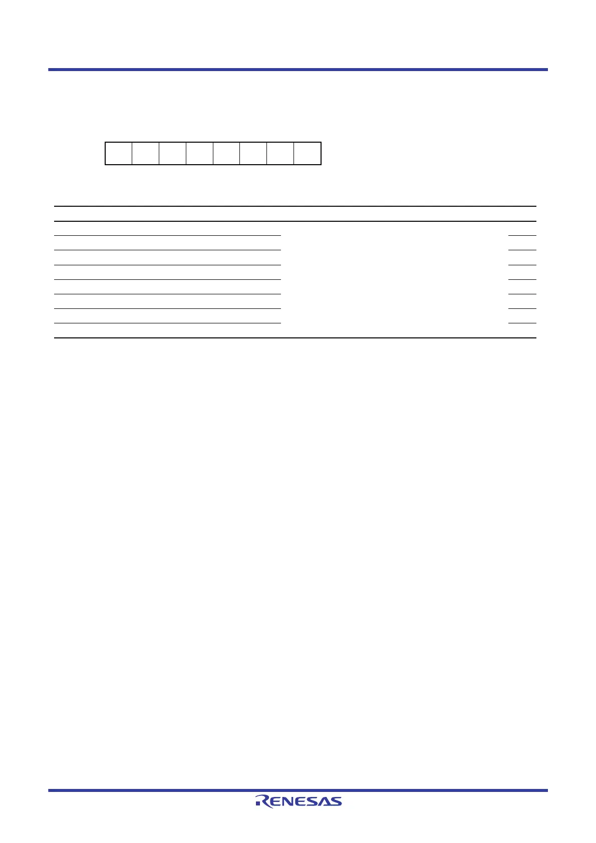
Address(es): ELC.PDBF1 0008 B127h, ELC.PDBF2 0008 B128h
b7 b6 b5 b4 b3 b2 b1 b0
PDBF7 PDBF6 PDBF5 PDBF4 PDBF3 PDBF2 PDBF1 PDBF0
Value after reset:
00000000
Bit Symbol Bit Name Description R/W
b0 PDBF0 Port Buffer 0 Specify the data to be transferred to the PODR register when
an event signal is input. The setting value is valid when the
PGCn.PGCO[2:0] bits are 011b or 1xxb. Write access to the
bit specified as a member of the input port group is disabled.
For details, refer to section 20.3, Operation.
R/W
b1 PDBF1 Port Buffer 1 R/W
b2 PDBF2 Port Buffer 2 R/W
b3 PDBF3 Port Buffer 3 R/W
b4 PDBF4 Port Buffer 4 R/W
b5 PDBF5 Port Buffer 5 R/W
b6 PDBF6 Port Buffer 6 R/W
b7 PDBF7 Port Buffer 7 R/W

 Loading...


