R01UH0823EJ0100 Rev.1.00 Page 1423 of 1823
Jul 31, 2019
RX23W Group 40. SD Host Interface (SDHIa)
40.2.2 Argument Register (SDARG)
The SDARG register is used for setting the argument field value. Set the SDARG register before setting the SDCMD
register. The argument field value of the automatically issued CMD12 is 0000 0000h regardless of the SDARG register
value.
40.2.3 Data Stop Register (SDSTOP)
Note 1. Do not rewrite this bit when the SDSTS2.CBSY flag is 1.
The SDSTOP register stops data transfer. During a multi-block transfer sequence, the SDBLKCNT register value
(number of blocks to be transferred) can be set to valid or invalid by setting the SDSTOP register.
STP Bit (Transfer Stop)
When setting the STP bit to 1, set it after the SDSTS1.RSPEND flag becomes 1; when setting the STP bit to 0, set it after
the SDSTS1.ACEND flag becomes 1. After a command sequence is complete, the SDHI does not issue CMD12 and the
SDSTS1.ACEND flag does not become 1 even if the STP bit is set to 1. When the SDHI is in the busy state after
receiving the R1b response, the SDHI does not issue CMD12 even if the STP bit is 1, and after the SDHI is released from
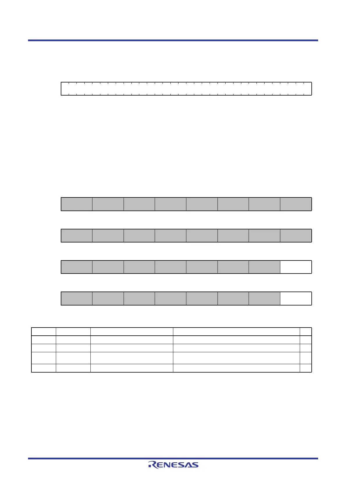
SDARG
Address(es): SDHI.SDARG 0008 AC08h
b31 b30 b29 b28 b27 b26 b25 b24 b23 b22 b21 b20 b19 b18 b17 b16 b15 b14 b13 b12 b11 b10 b9 b8 b7 b6 b5 b4 b3 b2 b1 b0
Value after reset:
00000000000000000000000000000000
SDSTOP
Address(es): SDSTOP 0008 AC10h
b31 b30 b29 b28 b27 b26 b25 b24
— — — — — — — —
Value after reset:
00000000
b23 b22 b21 b20 b19 b18 b17 b16
— — — — — — — —
Value after reset:
00000000
b15 b14 b13 b12 b11 b10 b9 b8
— — — — — — —
SDBLKCNTEN
Value after reset:
00000000
b7 b6 b5 b4 b3 b2 b1 b0
— — — — — — —STP
Value after reset:
00000000
Bit Symbol Bit Name Description R/W
b0 STP Transfer Stop Data transfer stops when this bit is set to 1. R/W
b7 to b1 — Reserved These bits are 0 when read and cannot be modified. R
b8 SDBLKCNTEN Block Count Register Value Select
*1
0: SDBLKCNT register value is invalid
1: SDBLKCNT register value is valid
R/W
b31 to b9 — Reserved These bits are 0 when read and cannot be modified. R

 Loading...


