R01UH0823EJ0100 Rev.1.00 Page 1023 of 1823
Jul 31, 2019
RX23W Group 33. Serial Communications Interface (SCIg, SCIh)
33.3.6 SCI Initialization (Asynchronous Mode)
Before transmitting and receiving data, start by writing the initial value 00h to the SCR register and then continue
through the procedure for SCI given in
Figure 33.8. Whenever the operating mode or transfer format is changed, the
SCR register must be initialized before the change is made.
When the external clock is used in asynchronous mode, ensure that the clock signal is supplied even during initialization.
Note that setting the SCR.RE bit to 0 initializes neither the ORER, FER, PER, and RDRF flags in the SSR register nor
registers RDR, RDRH, and RDRL.
Moreover, note that changing the value of the SCR.TE bit from 1 to 0 or 0 to 1 while the SCR.TIE bit is 1 leads to the
generation of a transmit data empty interrupt (TXI) request.
In addition, note that setting bits TIE, TE, and TEIE in the SCR register to 1 simultaneously leads to the generation of a
transmit end interrupt (TEI) request before the generation of a TXI interrupt request.
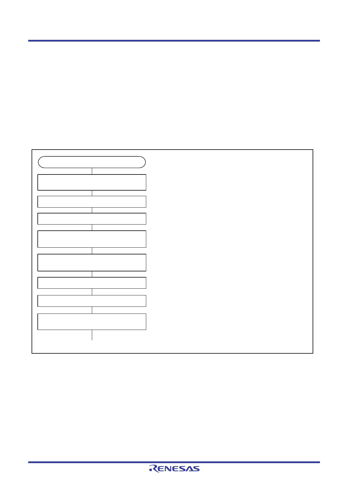
Figure 33.8 Sample SCI Initialization Flowchart (Asynchronous Mode)
Initialization completed
Start initialization
[ 1 ]
Set the SCR.TIE, RIE, TE, RE, and
TEIE bits to 0
[ 1 ] Make I/O port settings to enable input and output functions
as required for TXDn, RXDn, and SCKn pins.
[ 2 ] Set the clock selection in SCR.
When the clock output is selected in asynchronous mode,
the clock is output immediately after SCR settings are made.
[ 3 ] Set the SIMR1.IICM bit to 0.
Set the SPMR.CKPH and CKPOL bits to 0.
Step [3] can be skipped if the values have not been changed
from the initial values.
[ 4 ] Set data transmission/reception format in SMR, SCMR, and
SEMR.
[ 5 ] Write a value corresponding to the bit rate to BRR.
This step is not necessary if an external clock is used.
[ 6 ] Write the value obtained by correcting a bit rate error in
MDDR. This step is not necessary if the BRME bit in SEMR
is set to 0 or an external clock is used.
[ 7 ] Set the SCR.TE or RE bit to 1. Also set the SCR.TIE and
RIE bits.
Setting the TE and RE bits allows TXDn and RXDn to be
used.
Set the I/O port functions
[ 2 ]
[ 4 ]
[ 6 ]
[ 7 ]
Set the data transmission/reception format in
SMR, SCMR, and SEMR
Set a value in MDDR
Set the SCR.TE or RE bit to 1, and
set the SCR.TIE and RIE bits
Set the SCR.CKE[1:0] bits
Set the SIMR1.IICM bit to 0
Set the SPMR.CKPH and CKPOL bits to 0
[ 3 ]
[ 5 ]
Set a value in BRR

 Loading...


