R01UH0823EJ0100 Rev.1.00 Page 443 of 1823
Jul 31, 2019
RX23W Group 21. I/O Ports
21.3.3 Port Input Data Register (PIDR)
m = 0 to 4, B to E, J
PIDR indicates individual pin states of port m.
The pin states of port m can be read with the PORTm.PIDR, regardless of the values of PORTm.PDR and PORTm.PMR.
The NMI pin state is reflected in the P35 bit.
The bit corresponding to a pin that does not exist is reserved. A reserved bit is read as undefined, and cannot be modified.
Note: When using P36 and P37 as general I/O ports, set the MOSCCR.MOSTP bit to 1 (main clock oscillator is
stopped) and the P36 and P37 control bits in the PORT3.PMR register to 0 (use pin as general I/O port).
Address(es): PORT0.PIDR 0008 C040h, PORT1.PIDR 0008 C041h, PORT2.PIDR 0008 C042h, PORT3.PIDR 0008 C043h,
PORT4.PIDR 0008 C044h, PORTB.PIDR 0008 C04Bh, PORTC.PIDR 0008 C04Ch, PORTD.PIDR 0008 C04Dh,
PORTE.PIDR 0008 C04Eh, PORTJ.PIDR 0008 C052h
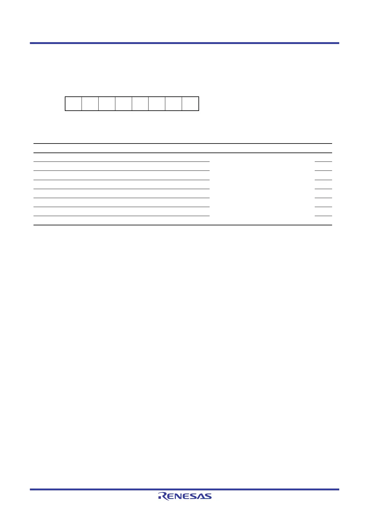
b7 b6 b5 b4 b3 b2 b1 b0
B7 B6 B5 B4 B3 B2 B1 B0
Value after reset:
xxxxxxxx
x: Undefined
Bit Symbol Bit Name Description R/W
b0 B0 Pm0 Indicates individual pin states of the
corresponding port.
R
b1 B1 Pm1 R
b2 B2 Pm2 R
b3 B3 Pm3 R
b4 B4 Pm4 R
b5 B5 Pm5 R
b6 B6 Pm6 R
b7 B7 Pm7 R

 Loading...


