R01UH0823EJ0100 Rev.1.00 Page 463 of 1823
Jul 31, 2019
RX23W Group 22. Multi-Function Pin Controller (MPC)
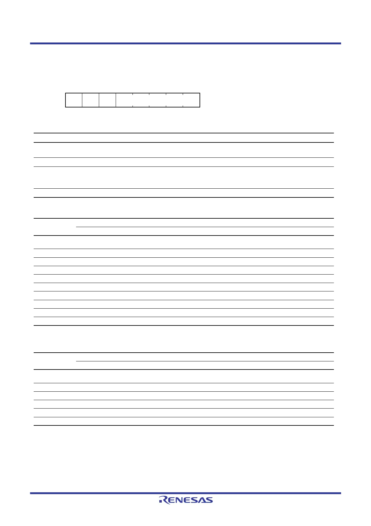
22.2.7 PBn Pin Function Control Registers (PBnPFS) (n = 0, 1, 3, 5, 7)
—: Do not specify this value.
—: Do not specify this value.
Address(es): PB0PFS 0008 C198h, PB1PFS 0008 C199h, PB3PFS 0008 C19Bh, PB5PFS 0008 C19Dh,
PB7PFS 0008 C19Fh
b7 b6 b5 b4 b3 b2 b1 b0
— ISEL — PSEL[4:0]
Value after reset:
00000000
Bit Symbol Bit Name Description R/W
b4 to b0 PSEL[4:0] Pin Function Select These bits select the peripheral function. For individual pin functions,
see the tables below.
R/W
b5 — Reserved This bit is read as 0. The write value should be 0. R/W
b6 ISEL Interrupt Input Function Select 0: Not used as IRQn input pin
1: Used as IRQn input pin
PB1: IRQ4 (85/56 pins)
R/W
b7 — Reserved This bit is read as 0. The write value should be 0. R/W
Table 22.7 Register Settings for Input/Output Pin Function in 85-Pin
PSEL[4:0]
Settings
Pin
PB0 PB1 PB3 PB5 PB7
00000b
(initial value)
Hi-Z
00001b — MTIOC0C MTIOC0A MTIOC2A MTIOC3B
00010b — MTIOC4C MTIOC4A MTIOC1B —
00011b TIOCA3 TIOCB3 TIOCD3 TIOCB4 TIOCB5
00100b — — TCLKD — —
00101b — TMCI0 TMO0 TMRI1 —
00111b — — POE3# POE1# —
01101b RSPCKA — — — —
10001b — — — USB0_VBUS —
11010b SDHI_CMD SDHI_CLK SDHI_WP SDHI_CD SDHI_D2
Table 22.8 Register Settings for Input/Output Pin Function in 56-Pin
PSEL[4:0]
Settings
Pin
PB0 PB1 PB7
00000b
(initial value)
Hi-Z
00001b — MTIOC0C MTIOC3B
00010b — MTIOC4C —
00011b TIOCA3 TIOCB3 TIOCB5
00101b — TMCI0 —
01101b RSPCKA — —

 Loading...


