R01UH0823EJ0100 Rev.1.00 Page 1626 of 1823
Jul 31, 2019
RX23W Group 45. 12-Bit D/A Converter (R12DAA)
45.3.1 Measure against Interference between D/A and A/D Conversion
When D/A conversion starts, an inrush current occurs to the 12-bit D/A converter. Since the same analog power supply is
shared by the 12-bit D/A converter and 12-bit A/D converter, the inrush current may interfere with the proper operation
of the 12-bit A/D converter.
With the DAADSCR.DAADST bit being 1, even if the DADRm register data (m = 0, 1) is modified during 12-bit A/D
converter operation, D/A conversion does not start immediately but starts synchronously with A/D conversion
completion. It takes a maximum of one A/D conversion time for the DADRm register data update to be reflected as the
D/A conversion circuit input. Before reflection, the DADRm register value does not correspond to the analog output
value.
When this function is enabled, it is impossible to check by any software means whether the DADRm register value has
been D/A converted or not.
Even with the DAADSCR.DAADST bit being 1, when the DADRm register data is modified while the 12-bit A/D
converter is halted, D/A conversion starts in one PCLKB cycle.
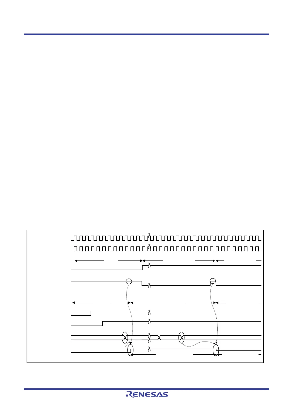
Figure 45.3 shows an example of channel 0 D/A conversion, in which the 12-bit D/A converter operates synchronously
with the 12-bit A/D converter.
(1) Confirm that the 12-bit A/D converter is halted. Set the DAADSCR.DAADST bit to 1.
(2) Confirm that the 12-bit A/D converter is halted. Set the DACR.DAOE0 bit to 1.
(3) Set the DADR0 register. When ADCLK is faster than the peripheral module clock, it may take longer than one A/D
conversion time.
If the 12-bit A/D conversion is halted (ADCSR.ADST bit = 0) when the DADR0 register is modified, D/A
conversion starts in one PCLKB cycle.
If the 12-bit A/D conversion is in progress (ADCSR.ADST bit = 1) when the DADR0 register is modified, D/A
conversion starts upon A/D conversion completion. If the DADR0 register is modified twice during A/D
conversion, the first update may not be converted.
Figure 45.3 Example of Conversion When the 12-Bit D/A Converter is Synchronized with the 12-Bit A/D
Converter
DAADSCR.DAADST bit
DADR0 register
DA0 output
A
C
PCLKB
12-bit A/D converter
synchronous D/A
conversion enable
signal (internal signal)
DACR.DAOE0 bit
ADST bit
B
(1)
(2)
(3)
(3) (3)
A/D conversion 2A/D conversion 1Halted
Standby D/A conversion A D/A conversion C
Post-D/A conversion
value C output
Post-D/A conversion
value A output
ADCLK
12-bit A/D conversion
12-bit D/A conversion

 Loading...


