R01UH0823EJ0100 Rev.1.00 Page 1494 of 1823
Jul 31, 2019
RX23W Group 43. Capacitive Touch Sensing Unit (CTSU)
43.2.2 CTSU Control Register 1 (CTSUCR1)
The CTSUCR1 register should be set when the CTSUCR0.CTSUSTRT bit is 0.
CTSUPON Bit (CTSU Power Supply Enable)
This bit controls power supply to the CTSU. Set the CTSUPON and CTSUCSW bits to the same value at the same time.
CTSUCSW Bit (CTSU LPF Capacitance Charging Control)
This bit controls charging of the LPF capacitor connected to the TSCAP pin (turning on/off of the capacitance switch).
After the capacitance switch is turned on, wait until the capacitance connected to the TSCAP pin is charged for the
specified time before starting measurement (CTSUCR0.CTSUSTRT = 1). Prior to measurement, use an I/O port to
output a low level to the TSCAP pin, and discharge the LPF capacitance that has been already charged. Set the
CTSUPON and CTSUCSW bits to the same value at the same time.
CTSUATUNE0 Bit (CTSU Power Supply Operating Mode Setting)
This bit sets the power supply operating mode. Set this bit according to the lower limit of the VCC for operating the
CTSU. As an example, when performing touch measurement in a system (the VCC voltage range is 2 to 3 V) where the
VCC varies depending on battery operation, set this bit to 1 regardless of the initial VCC voltage.
CTSUATUNE1 Bit (CTSU Power Supply Capacity Adjustment)
This bit sets the capacity of the CTSU power supply. Normally, the value of this bit should be set to 0.
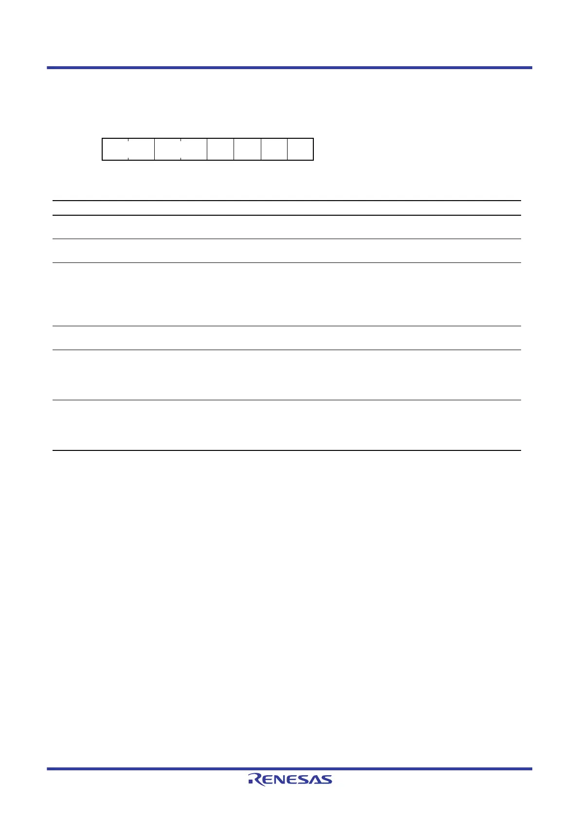
Address(es): CTSU.CTSUCR1 000A 0901h
b7 b6 b5 b4 b3 b2 b1 b0
CTSUMD[1:0] CTSUCLK[1:0]
CTSUA
TUNE1
CTSUA
TUNE0
CTSUC
SW
CTSUP
ON
Value after reset:
00000 000
Bit Symbol Bit Name Description R/W
b0 CTSUPON CTSU Power Supply Enable 0: Powered off
1: Powered on
R/W
b1 CTSUCSW CTSU LPF Capacitance Charging
Control
0: Capacitance switch turned off
1: Capacitance switch turned on
R/W
b2 CTSUATUNE0 CTSU Power Supply Operating Mode
Setting
VCC ≥ 2.4 V
0: Normal operating mode
1: Low-voltage operating mode
VCC < 2.4 V
0: Setting prohibited
1: Low-voltage operating mode
R/W
b3 CTSUATUNE1 CTSU Power Supply Capacity
Adjustment
0: Normal output
1: High-current output
R/W
b5, b4 CTSUCLK[1:0] CTSU Operating Clock Select
b5 b4
0 0: PCLK
0 1: PCLK/2 (PCLK divided by 2)
1 0: PCLK/4 (PCLK divided by 4)
1 1: Setting prohibited
R/W
b7, b6 CTSUMD[1:0] CTSU Measurement Mode Select
b7 b6
0 0: Self-capacitance single scan mode
0 1: Self-capacitance multi-scan mode
1 0: Setting prohibited
1 1: Mutual capacitance full scan mode
R/W

 Loading...


