R01UH0823EJ0100 Rev.1.00 Page 1065 of 1823
Jul 31, 2019
RX23W Group 33. Serial Communications Interface (SCIg, SCIh)
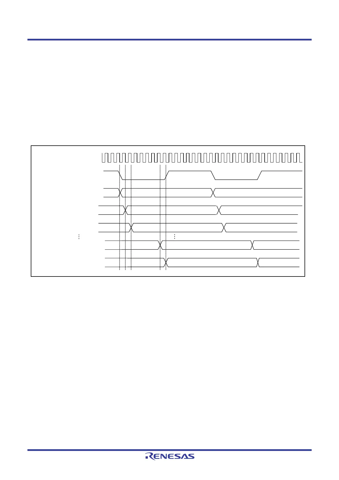
33.7.3 SSDA Output Delay
The IICDL[4:0] bits in the SIMR1 register can be used to set a delay for output on the SSDAn pin relative to falling
edges of output on the SSCLn pin. Delay-time settings from 0 to 31 are selectable, representing periods of the
corresponding numbers of cycles of the clock signal from the on-chip baud rate generator (derived by frequency-dividing
the base clock, PCLK, by the divisor selected by the CKS[1:0] bits in the SMR register). A delay for output on the
SSDAn pin is for the start condition/restart condition/stop condition signal, 8-bit transmit data, and an acknowledge bit.
If the SSDA output delay is shorter than the time for the level on the SSCLn pin to fall, the change of the output on the
SSDAn pin will start while the output level on the SSCLn pin is falling, creating a possibility of erroneous operation for
slave devices. Ensure that settings for the delay of output on the SSDAn pin are for times greater than the time output on
the SSCLn pin takes to fall (300 ns for I
2
C-bus in normal mode and fast mode).
Figure 33.50 shows the timing of delays in SSDA output.
Figure 33.50 Timing of Delays in SSDA Output
Output on the SSCLn pin
Clock signal from the on-chip
baud rate generator (internal signal)
Output on the SSDAn pin
(IICDL[4:0] = 00000b)
Output on the SSDAn pin
(IICDL[4:0] = 00001b)
Output on the SSDAn pin
(IICDL[4:0] = 00010b)
Output on the SSDAn pin
(IICDL[4:0] = 00111b)
Output on the SSDAn pin
(IICDL[4:0] = 01000b)

 Loading...


