R01UH0823EJ0100 Rev.1.00 Page 153 of 1823
Jul 31, 2019
RX23W Group 7. Option-Setting Memory (OFSM)
7.2.2 Option Function Select Register 1 (OFS1)
Note 1. Set the same value to this address when using start-up program protection.
Note 2. The value of the blank product is FFFF FFFFh. This register is set to a specified value after programming of the flash memory
with the user program.
The OFS1 register is allocated in the ROM. Set this register at the same time as writing the program. After writing, do
not write additions to this register.
When erasing the block including the OFS1 register, the OFS1 register value becomes FFFF FFFFh.
The setting in the OFS1 register is ignored in boot mode, and this register functions similarly when it is set to FFFF
FFFFh.
VDSEL[1:0] Bits (Voltage Detection 0 Level Select)
These bits select the voltage detection level to be monitored by the voltage detection 0 circuit.
Set the voltage detection 0 level to 2.51 V (set VDSEL[1:0] bits to 10b) before using the battery backup function (setting
the VBATTCR.VBATTDIS bit to 0).
LVDAS Bit (Voltage Detection 0 Circuit Start)
This bit selects whether the voltage monitoring 0 reset is enabled or disabled after a reset.
The Vdet0 voltage to be monitored by the voltage detection 0 circuit is selected by the VDSEL[1:0] bits.
FASTSTUP Bit (Power-On Fast Startup Time)
The startup time can be reduced by setting this bit to 0 (fast startup time at power on) when it is possible to meet the
power-on VCC rising gradient (during fast startup time) shown in Electrical Characteristics. Do not set this bit to 0 when
it is not possible to meet the power-on VCC rising gradient (during fast startup time).
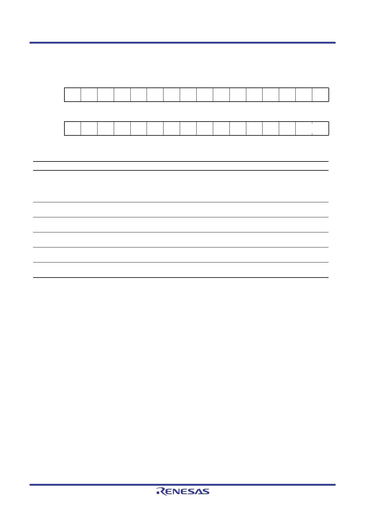
Address(es):
OFSM.OFS1 FFFF FF88h, (FFFF 7F88h)*
1
b31 b30 b29 b28 b27 b26 b25 b24 b23 b22 b21 b20 b19 b18 b17 b16
————————————————
Value after reset:
The value set by the user*
2
b15 b14 b13 b12 b11 b10 b9 b8 b7 b6 b5 b4 b3 b2 b1 b0
———————
HOCO
EN
————
FASTS
TUP
LVDAS VDSEL[1:0]
Value after reset:
The value set by the user*
2
Bit Symbol Bit Name Description R/W
b1, b0 VDSEL[1:0] Voltage Detection 0 Level
Select
b1 b0
0 0: Settings prohibited
0 1: 2.82 V is selected
1 0: 2.51 V is selected
1 1: 1.90 V is selected
R
b2 LVDAS Voltage Detection 0 Circuit
Start
0: Voltage monitoring 0 reset is enabled after a reset
1: Voltage monitoring 0 reset is disabled after a reset
R
b3 FASTSTUP Power-On Fast Startup Time 0: Fast startup time at power on
1: Normal startup
R
b7 to b4 — Reserved When reading, these bits return the value written by the user.
The write value should be 1.
R
b8 HOCOEN HOCO Oscillation Enable 0: HOCO oscillation is enabled after a reset
1: HOCO oscillation is disabled after a reset
R
b31 to b9 — Reserved When reading, these bits return the value written by the user.
The write value should be 1.
R

 Loading...


