R01UH0823EJ0100 Rev.1.00 Page 1060 of 1823
Jul 31, 2019
RX23W Group 33. Serial Communications Interface (SCIg, SCIh)
33.6.8 Clock Output Control
Clock output can be fixed to high or low using the SCR.CKE[1:0] bits when the SMR.GM bit is 1. When the CKE[1:0]
bits are set to 01b (clock output), the base clock is output from the SCK pin. For the settings of the base clock frequency
(bit rate), refer to
section 33.2.11, Bit Rate Register (BRR). When the CKE[1:0] bits are set to 00b (output fixed low)
or 10b (output fixed to high), the SCK pin can be fixed to low or high.
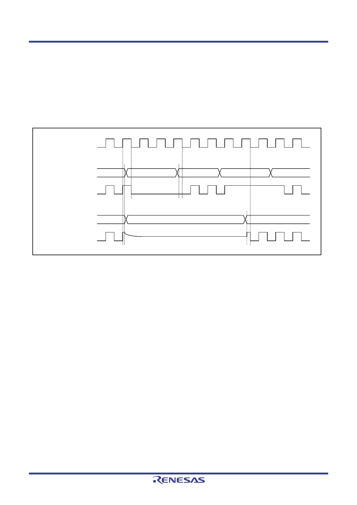
Figure 33.45 shows a timing chart when the clock output is controlled.
If changing the CKE[1:0] bits while the SMR.GM bit is 0 (non-GSM mode), a pulse of unexpected width may output
from SCK pin because the result is immediately reflected to the SCK pin.
Figure 33.45 Clock Output Control
Base clock
SCR.CKE[1:0] bits
01b 00b 01b
SCR.CKE[1:0] bits 01b 00b 01b 10b 01b
When the SCR.GM bit is 0
When the SCR.GM bit is 1
SCK
SCK
Hi-Z

 Loading...


