R01UH0823EJ0100 Rev.1.00 Page 1705 of 1823
Jul 31, 2019
RX23W Group 50. Flash Memory (FLASH)
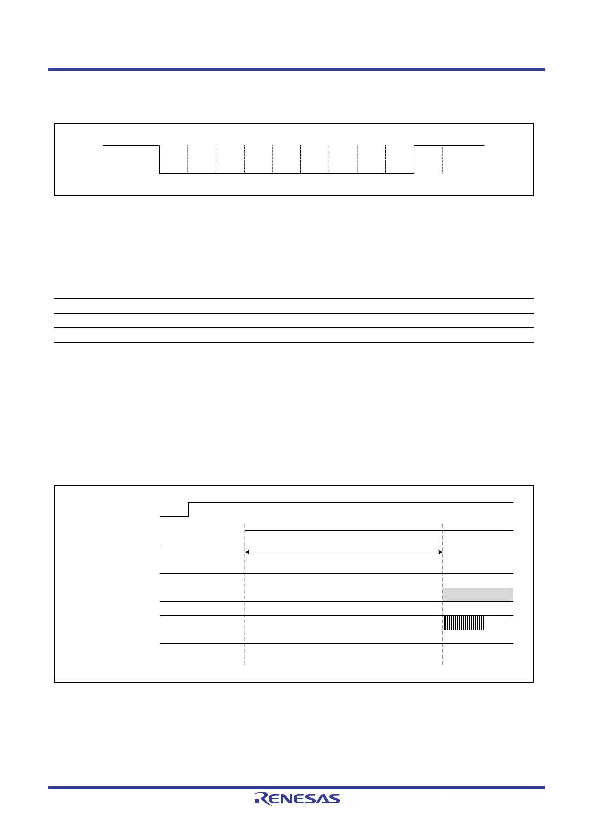
As shown in Figure 50.25, set the format to 8-bit data, 1 stop bit, no parity, and LSB first to communicate with the serial
programmer.
Figure 50.25 Communication Format
Initial communication with the programmer is performed at 9,600 or 19,200 bps. The communication bit rate can be
changed after the MCU is connected with the programmer.
Table 50.11 lists the maximum communication bit rates for communication in boot mode (SCI interface).
50.8.2.2 Starting Up in Boot Mode (SCI Interface)
To start the MCU in boot mode (SCI interface), a reset must be released by changing the RES# pin from low to high
while both of the MD pin and UB pin are low. After starting up in boot mode (SCI interface), wait at least 400 ms until
communication with the MCU is enabled in boot mode (SCI interface).
As shown in
Figure 50.26, keep the signal of each pin unchanged for 400 ms after the reset is released. Use resets
according to the range described in
section 51.3.2, Reset Timing.
Figure 50.26 Wait Time until Communication Becomes Possible in Boot Mode (SCI Interface)
Table 50.11 Conditions for Communication
Operating Voltage Maximum Communication Bit Rate
Lower than 3.0 V 500 kbps
3.0 V or higher 2 Mbps
Start
bit
D0 D1 D2 D3 D4 D5 D6 D7
Stop
bit
System power supply
RES#
MD
UB
RXD1
TXD1
Low or open
Low
High
High
Communication starts
400 ms or longer

 Loading...


