R01UH0823EJ0100 Rev.1.00 Page 1673 of 1823
Jul 31, 2019
RX23W Group 50. Flash Memory (FLASH)
50.4.13 Flash Processing End Address Register H (FEARH)
The FEARH register is used to set the end address of the target processing range in the flash memory when a software
command is executed.
Set bit 31 to bit 25 and bit 20 to bit 16 of the flash memory address for programming/erasure in this register.
Data can be written to this register in ROM P/E mode or E2 DataFlash P/E mode.
This register is initialized by a reset or setting the FRESETR.FRESET bit to 1. Data cannot be written to this register
while the FRESETR.FRESET bit is 1.
If this register is read while executing a software command set by the FEXCR register, an undefined value is read.
Refer to
Figure 50.1 and Figure 50.2 for details on the addresses of the flash memory.
50.4.14 Flash Processing End Address Register L (FEARL)
The FEARH register is used to set the end address of the target range for processing when a software command is
executed.
Set bit 15 to bit 0 of the flash memory address for programming/erasure in this register.
When the target is the ROM, set bit 2 to bit 0 to 000b.
Data can be written to this register in ROM P/E mode or E2 DataFlash P/E mode.
This register is initialized by a reset or setting the FRESETR.FRESET bit to 1. Data cannot be written to this register
while the FRESETR.FRESET bit is 1.
If this register is read while executing a software command set by the FEXCR register, an undefined value is read.
Refer to
Figure 50.1 and Figure 50.2 for details on the addresses of the flash memory.
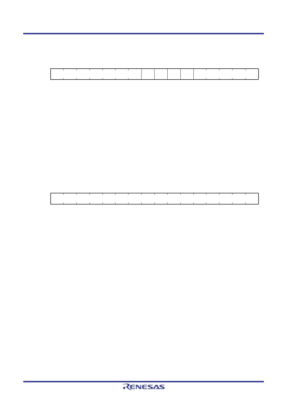
Address(es): FLASH.FEARH 007F C120h
b15 b14 b13 b12 b11 b10 b9 b8 b7 b6 b5 b4 b3 b2 b1 b0
————
Value after reset:
0000000000000000
Address(es): FLASH.FEARL 007F C118h
b15 b14 b13 b12 b11 b10 b9 b8 b7 b6 b5 b4 b3 b2 b1 b0
Value after reset:
0000000000000000

 Loading...


